JAJSBU0F July 2012 – November 2020 TPS54020
PRODUCTION DATA
- 1 特長
- 2 アプリケーション
- 3 概要
- 4 Revision History
- 5 Description (Continued)
- 6 Pin Configuration and Functions
- 7 Specifications
-
8 Detailed Description
- 8.1 Overview
- 8.2 Functional Block Diagram
- 8.3
Feature Description
- 8.3.1 Fixed Frequency PWM Control
- 8.3.2 Input Voltage and Power Input Voltage Pins (VIN and PVIN)
- 8.3.3 Voltage Reference (VREF)
- 8.3.4 Adjusting the Output Voltage
- 8.3.5 Safe Start-up into Prebiased Outputs
- 8.3.6 Error Amplifier
- 8.3.7 Slope Compensation
- 8.3.8 Enable and Adjusting Undervoltage Lockout
- 8.3.9 Adjustable Switching Frequency and Synchronization (RT/CLK)
- 8.3.10 Soft-Start (SS) Sequence
- 8.3.11 Power Good (PWRGD)
- 8.3.12 Bootstrap Voltage (BOOT) and Low Dropout Operation
- 8.3.13 Sequencing (SS)
- 8.3.14 Output Overvoltage Protection (OVP)
- 8.3.15 Overcurrent Protection
- 8.3.16 Thermal Shutdown
- 8.4 Device Functional Modes
-
9 Application and Implementation
- 9.1 Application Information
- 9.2
Typical Application
- 9.2.1 Design Requirements
- 9.2.2
Detailed Design Procedure
- 9.2.2.1 Custom Design With WEBENCH® Tools
- 9.2.2.2 Operating Frequency
- 9.2.2.3 Output Inductor Selection
- 9.2.2.4 Output Capacitor Selection
- 9.2.2.5 Input Capacitor Selection
- 9.2.2.6 Soft-Start Capacitor Selection
- 9.2.2.7 Bootstrap Capacitor Selection
- 9.2.2.8 Undervoltage Lockout Set Point
- 9.2.2.9 Output Voltage Feedback Resistor Selection
- 9.2.2.10 Compensation Component Selection
- 9.2.3 Application Curves
- 10Power Supply Recommendations
- 11Layout
- 12Device and Documentation Support
- 13Mechanical, Packaging, and Orderable Information
パッケージ・オプション
メカニカル・データ(パッケージ|ピン)
- RUW|15
サーマルパッド・メカニカル・データ
- RUW|15
発注情報
9.1.2 Simple Small Signal Model for Peak Current Mode Control
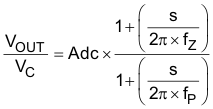
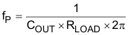
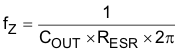
Figure 9-2 is a small signal model that can be used to understand how to design the frequency compensation network. This is a simplified model that does not include the effects of slope compensation. The device power stage, or Plant, can be approximated by a voltage controlled current source (duty cycle modulator) supplying current to the output capacitor and load resistor. The control to output transfer function is shown in Equation 10 and consists of a dc gain, one dominant pole and one ESR zero. The quotient of the change in switch current and the change in COMP pin voltage (node c in Figure 9-1) is the power stage transconductance (gmps) which is 20 A/V for the TPS54020 (when ILIM is open). The DC gain or amplification of the power stage, ADC, is the product of gmps and the load resistance RL as shown in Equation 11 with resistive loads. As the load current increases, the DC gain decreases. This variation with load may seem problematic at first glance, but fortunately the dominant pole moves with load current (see Equation 12). The combined effect is highlighted by the dashed line in Figure 9-3. As the load current decreases, the gain increases and the pole frequency reduces, keeping the 0-dB crossover frequency the same for the varying load conditions which makes it easier to design the frequency compensation.
 Figure 9-2 Simplified Small Signal Model for Peak Current Mode Control
 Figure 9-3 Simplified Frequency Response for Peak Current Mode Control
The simplified control-to-output transfer function is shown in Equation 10.
The power stage DC gain is shown in Equation 11.

The pole from load is show in Equation 12.
To calculate the zero from the capacitor ESR use Equation 13.
where
- gM(ea) is the transconductance amplifier gain (1300 μA/V)
- gM(ps) is the power stage gain (20 A/V)
- RLOAD is the load resistance
- COUT is the output capacitance
- RESR is the equivalent series resistance of the output capacitor