JAJSBU0F July 2012 – November 2020 TPS54020
PRODUCTION DATA
- 1 特長
- 2 アプリケーション
- 3 概要
- 4 Revision History
- 5 Description (Continued)
- 6 Pin Configuration and Functions
- 7 Specifications
-
8 Detailed Description
- 8.1 Overview
- 8.2 Functional Block Diagram
- 8.3
Feature Description
- 8.3.1 Fixed Frequency PWM Control
- 8.3.2 Input Voltage and Power Input Voltage Pins (VIN and PVIN)
- 8.3.3 Voltage Reference (VREF)
- 8.3.4 Adjusting the Output Voltage
- 8.3.5 Safe Start-up into Prebiased Outputs
- 8.3.6 Error Amplifier
- 8.3.7 Slope Compensation
- 8.3.8 Enable and Adjusting Undervoltage Lockout
- 8.3.9 Adjustable Switching Frequency and Synchronization (RT/CLK)
- 8.3.10 Soft-Start (SS) Sequence
- 8.3.11 Power Good (PWRGD)
- 8.3.12 Bootstrap Voltage (BOOT) and Low Dropout Operation
- 8.3.13 Sequencing (SS)
- 8.3.14 Output Overvoltage Protection (OVP)
- 8.3.15 Overcurrent Protection
- 8.3.16 Thermal Shutdown
- 8.4 Device Functional Modes
-
9 Application and Implementation
- 9.1 Application Information
- 9.2
Typical Application
- 9.2.1 Design Requirements
- 9.2.2
Detailed Design Procedure
- 9.2.2.1 Custom Design With WEBENCH® Tools
- 9.2.2.2 Operating Frequency
- 9.2.2.3 Output Inductor Selection
- 9.2.2.4 Output Capacitor Selection
- 9.2.2.5 Input Capacitor Selection
- 9.2.2.6 Soft-Start Capacitor Selection
- 9.2.2.7 Bootstrap Capacitor Selection
- 9.2.2.8 Undervoltage Lockout Set Point
- 9.2.2.9 Output Voltage Feedback Resistor Selection
- 9.2.2.10 Compensation Component Selection
- 9.2.3 Application Curves
- 10Power Supply Recommendations
- 11Layout
- 12Device and Documentation Support
- 13Mechanical, Packaging, and Orderable Information
パッケージ・オプション
メカニカル・データ(パッケージ|ピン)
- RUW|15
サーマルパッド・メカニカル・データ
- RUW|15
発注情報
9.2.2.10 Compensation Component Selection
There are several industry techniques used to compensate DC/DC regulators. The method presented here is easy to calculate and yields high phase margins. For most conditions, the regulator has a phase margin between 60 and 90 degrees. The method presented here ignores the effects of the slope compensation that is internal to the TPS54020. Because the slope compensation is ignored, the actual cross over frequency is usually lower than the cross over frequency used in the calculations. Use the PSPICE model for a more accurate design.
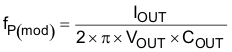
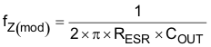
First, the modulator pole, fP(mod), and the esr zero, fZ(mod), must be calculated using Equation 30 and Equation 31.
For the output capacitance, use a derated value of 225 μF. As a quick estimate, an fC value between three and five times the double pole frequency of the output filter is chosen. In this case, an fC of 35 kHz was selected. fP(mod) is 3.93 kHz and fZ(mod) is 10.6 MHz.
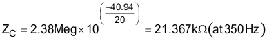
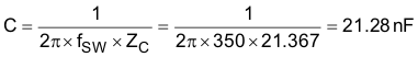
Now the compensation components can be calculated. First, calculate the value for C12 which sets the gain of the compensated network at low frequencies far below fC. Because the desired fC is 35 kHz, and the expected gain curve is a single pole roll off, two decades below fC (which is 350 Hz), the gain should be +40 dB. Following this logic, the plant gain at DC is calculated in Equation 32.
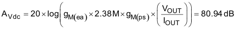
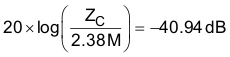
This implies that at 350 Hz, the compensation pole capacitor C12 should reduce the gain by (80.94-40) =
40.94 dB, or result in a gain of -40.94 dB. (See Equation 33)
where
- fSW is in kHz
The closest standard value is 22 nF.
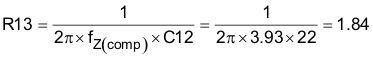
From Equation 30, the required compensation zero resulting from R13 should be placed at fP(mod) of 3.93 kHz.
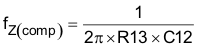
where
- fZ(comp) is in kHz
- C12 is in nF
- R13 is in kΩ
This value was adjusted after actual Bode measurements to 3.01 kΩ.
An additional high frequency pole can be used if necessary by adding a capacitor in parallel with the series combination of R13 and C12. The pole frequency can be placed at the ESR zero frequency of the output capacitor as given by Equation 13. Use Equation 38 to calculate the required capacitor value for C10.
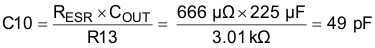
This value was adjusted upwards to 22 0pF to reduce jitter.