JAJSOW5F April 2006 – January 2024 TPS5420
PRODUCTION DATA
- 1
- 1特長
- 2アプリケーション
- 3概要
- 4静電気放電に関する注意事項
- 5Ordering Information
- 6Pin Assignments
- 7Specifications
-
8Application Information
- 8.1 Functional Block Diagram
- 8.2
Detailed Description
- 8.2.1 Oscillator Frequency
- 8.2.2 Voltage Reference
- 8.2.3 Enable (ENA) and Internal Slow Start
- 8.2.4 Undervoltage Lockout (UVLO)
- 8.2.5 Boost Capacitor (BOOT)
- 8.2.6 Output Feedback (VSENSE)
- 8.2.7 Internal Compensation
- 8.2.8 Voltage Feed Forward
- 8.2.9 Pulse-Width-Modulation (PWM) Control
- 8.2.10 Overcurrent Limiting
- 8.2.11 Overvoltage Protection
- 8.2.12 Thermal Shutdown
- 8.2.13 PCB Layout
- 8.2.14 Application Circuits
- 8.2.15
Design Procedure
- 8.2.15.1 Design Parameters
- 8.2.15.2 Switching Frequency
- 8.2.15.3 Input Capacitors
- 8.2.15.4 Output Filter Components
- 8.2.15.5 Output Voltage Setpoint
- 8.2.15.6 Boot Capacitor
- 8.2.15.7 Catch Diode
- 8.2.15.8 Additional Circuits
- 8.2.15.9 Circuit Using Ceramic Output Filter Capacitors
- 8.2.15.10 Output Filter Component Selection
- 8.2.15.11 External Compensation Network
- 8.3 Advanced Information
- 8.4 Performance Graphs
- 9Revision History
8.3.2 Internal Compensation Network
The design equations given in the example circuit can be used to generate circuits using the TPS5420. These designs are based on certain assumptions, and always select output capacitors within a limited range of ESR values. If a different capacitor type is desired, it may be possible to fit one to the internal compensation of the TPS5420. Equation 23 gives the nominal frequency response of the internal voltage-mode type III compensation network:
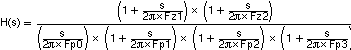
Where
Fp0 = 2165 Hz, Fz1 = 2170 Hz, Fz2 = 2590 Hz
Fp1 = 24 kHz, Fp2 = 54 kHz, Fp3 = 440 kHz
Fp3 represents the non-ideal parasitics effect.
Using this information along with the desired output voltage, feed forward gain and output filter characteristics, the closed loop transfer function can be derived.