JAJSOW5F April 2006 – January 2024 TPS5420
PRODUCTION DATA
- 1
- 1特長
- 2アプリケーション
- 3概要
- 4静電気放電に関する注意事項
- 5Ordering Information
- 6Pin Assignments
- 7Specifications
-
8Application Information
- 8.1 Functional Block Diagram
- 8.2
Detailed Description
- 8.2.1 Oscillator Frequency
- 8.2.2 Voltage Reference
- 8.2.3 Enable (ENA) and Internal Slow Start
- 8.2.4 Undervoltage Lockout (UVLO)
- 8.2.5 Boost Capacitor (BOOT)
- 8.2.6 Output Feedback (VSENSE)
- 8.2.7 Internal Compensation
- 8.2.8 Voltage Feed Forward
- 8.2.9 Pulse-Width-Modulation (PWM) Control
- 8.2.10 Overcurrent Limiting
- 8.2.11 Overvoltage Protection
- 8.2.12 Thermal Shutdown
- 8.2.13 PCB Layout
- 8.2.14 Application Circuits
- 8.2.15
Design Procedure
- 8.2.15.1 Design Parameters
- 8.2.15.2 Switching Frequency
- 8.2.15.3 Input Capacitors
- 8.2.15.4 Output Filter Components
- 8.2.15.5 Output Voltage Setpoint
- 8.2.15.6 Boot Capacitor
- 8.2.15.7 Catch Diode
- 8.2.15.8 Additional Circuits
- 8.2.15.9 Circuit Using Ceramic Output Filter Capacitors
- 8.2.15.10 Output Filter Component Selection
- 8.2.15.11 External Compensation Network
- 8.3 Advanced Information
- 8.4 Performance Graphs
- 9Revision History
The maximum ESR of the output capacitor also determines the amount of output ripple as specified in the initial design parameters. The output ripple voltage is the inductor ripple current times the ESR of the output filter. Check that the maximum specified ESR as listed in the capacitor data sheet results in an acceptable output ripple voltage:
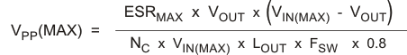
Where:
ΔVPP is the desired peak-to-peak output ripple.
NC is the number of parallel output capacitors.
FSW is the switching frequency.
The minimum ESR of the output capacitor should also be considered. For a good phase margin, if the ESR is zero when the ESR is at its minimum, it should not be above the internal compensation poles at 24 kHz and 54 kHz.
The selected output capacitor must also be rated for a voltage greater than the desired output voltage plus one half the ripple voltage. Any derating amount must also be included. The maximum RMS ripple current in the output capacitor is given by Equation 11:
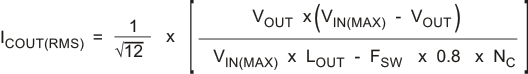
Where:
NC is the number of output capacitors in parallel.
FSW is the switching frequency.