SLVSFN6 December 2020 TPS54622-EP
PRODUCTION DATA
- 1 Features
- 2 Applications
- 3 Description
- 4 Revision History
- 5 Pin Configurations and Functions
- 6 Specifications
-
7 Detailed Description
- 7.1 Overview
- 7.2 Functional Block Diagram
- 7.3
Feature Description
- 7.3.1 Fixed-Frequency PWM Control
- 7.3.2 Continuous Current Mode Operation (CCM)
- 7.3.3 VIN and Power VIN Pins (VIN and PVIN)
- 7.3.4 Voltage Reference
- 7.3.5 Adjusting the Output Voltage
- 7.3.6 Safe Start-Up Into Prebiased Outputs
- 7.3.7 Error Amplifier
- 7.3.8 Slope Compensation
- 7.3.9 Enable and Adjusting Undervoltage Lockout
- 7.3.10 Adjustable Switching Frequency and Synchronization (RT/CLK)
- 7.3.11 Slow Start (SS/TR)
- 7.3.12 Power Good (PWRGD)
- 7.3.13 Output Overvoltage Protection (OVP)
- 7.3.14 Overcurrent Protection
- 7.3.15 Thermal Shutdown
- 7.3.16 Small Signal Model for Loop Response
- 7.3.17 Simple Small Signal Model for Peak Current Mode Control
- 7.3.18 Small Signal Model for Frequency Compensation
- 7.4 Device Functional Modes
-
8 Application and Implementation
- 8.1 Application Information
- 8.2
Typical Application
- 8.2.1 Design Requirements
- 8.2.2
Detailed Design Procedures
- 8.2.2.1 Custom Design With WEBENCH® Tools
- 8.2.2.2 Operating Frequency
- 8.2.2.3 Output Inductor Selection
- 8.2.2.4 Output Capacitor Selection
- 8.2.2.5 Input Capacitor Selection
- 8.2.2.6 Slow-Start Capacitor Selection
- 8.2.2.7 Bootstrap Capacitor Selection
- 8.2.2.8 Undervoltage Lockout Setpoint
- 8.2.2.9 Output Voltage Feedback Resistor Selection
- 8.2.2.10 Compensation Component Selection
- 8.2.2.11 Fast Transient Considerations
- 8.2.3 Application Curves
- 9 Power Supply Recommendations
- 10Layout
- 11Device and Documentation Support
- 12Mechanical, Packaging, and Orderable Information
7.3.17 Simple Small Signal Model for Peak Current Mode Control
Figure 7-5 is a simple small signal model that can be used to understand how to design the frequency compensation. The device power stage can be approximated to a voltage controlled current source (duty cycle modulator) supplying current to the output capacitor and load resistor. The control to output transfer function is shown in Equation 5 and consists of a DC gain, one dominant pole and one ESR zero. The quotient of the change in switch current and the change in COMP pin voltage (node c in Figure 7-4) is the power stage transconductance (gmps) which is 16 A/V for the device. The DC gain of the power stage is the product of gmps and the load resistance RL) as shown in Equation 6 with resistive loads. As the load current increases, the DC gain decreases. This variation with load may seem problematic at first glance, but fortunately the dominant pole moves with load current (see Equation 7). The combined effect is highlighted by the dashed line in Figure 7-6. As the load current decreases, the gain increases and the pole frequency lowers, keeping the 0-dB crossover frequency the same for the varying load conditions which makes it easier to design the frequency compensation.
 Figure 7-5 Simplified Small Signal Model for Peak Current Mode Control
 Figure 7-6 Simplified Frequency Response for Peak Current Mode Control
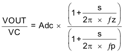
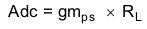
where
- gmps is the power stage gain (16 A/V).
- RL is the load resistance.
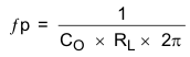
where
- CO is the output capacitance.
- RL is the load resistance.
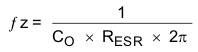
where
- CO is the output capacitance.
- RESR is the equivalent series resistance of the output capacitor.