SLVSFN6 December 2020 TPS54622-EP
PRODUCTION DATA
- 1 Features
- 2 Applications
- 3 Description
- 4 Revision History
- 5 Pin Configurations and Functions
- 6 Specifications
-
7 Detailed Description
- 7.1 Overview
- 7.2 Functional Block Diagram
- 7.3
Feature Description
- 7.3.1 Fixed-Frequency PWM Control
- 7.3.2 Continuous Current Mode Operation (CCM)
- 7.3.3 VIN and Power VIN Pins (VIN and PVIN)
- 7.3.4 Voltage Reference
- 7.3.5 Adjusting the Output Voltage
- 7.3.6 Safe Start-Up Into Prebiased Outputs
- 7.3.7 Error Amplifier
- 7.3.8 Slope Compensation
- 7.3.9 Enable and Adjusting Undervoltage Lockout
- 7.3.10 Adjustable Switching Frequency and Synchronization (RT/CLK)
- 7.3.11 Slow Start (SS/TR)
- 7.3.12 Power Good (PWRGD)
- 7.3.13 Output Overvoltage Protection (OVP)
- 7.3.14 Overcurrent Protection
- 7.3.15 Thermal Shutdown
- 7.3.16 Small Signal Model for Loop Response
- 7.3.17 Simple Small Signal Model for Peak Current Mode Control
- 7.3.18 Small Signal Model for Frequency Compensation
- 7.4 Device Functional Modes
-
8 Application and Implementation
- 8.1 Application Information
- 8.2
Typical Application
- 8.2.1 Design Requirements
- 8.2.2
Detailed Design Procedures
- 8.2.2.1 Custom Design With WEBENCH® Tools
- 8.2.2.2 Operating Frequency
- 8.2.2.3 Output Inductor Selection
- 8.2.2.4 Output Capacitor Selection
- 8.2.2.5 Input Capacitor Selection
- 8.2.2.6 Slow-Start Capacitor Selection
- 8.2.2.7 Bootstrap Capacitor Selection
- 8.2.2.8 Undervoltage Lockout Setpoint
- 8.2.2.9 Output Voltage Feedback Resistor Selection
- 8.2.2.10 Compensation Component Selection
- 8.2.2.11 Fast Transient Considerations
- 8.2.3 Application Curves
- 9 Power Supply Recommendations
- 10Layout
- 11Device and Documentation Support
- 12Mechanical, Packaging, and Orderable Information
7.3.9 Enable and Adjusting Undervoltage Lockout
The EN pin provides electrical on/off control of the device. Once the EN pin voltage exceeds the threshold voltage, the device starts operation. If the EN pin voltage is pulled below the threshold voltage, the regulator stops switching and enters low Iq state.
The EN pin has an internal pullup current source, allowing the user to float the EN pin for enabling the device. If an application requires controlling the EN pin, use open-drain or open collector output logic to interface with the pin.
The device implements internal UVLO circuitry on the VIN pin. The device is disabled when the VIN pin voltage falls below the internal VIN UVLO threshold. The internal VIN UVLO threshold has a hysteresis of 150 mV.
If an application requires either a higher UVLO threshold on the VIN pin or a secondary UVLO on the PVIN, in split rail applications, then the EN pin can be configured as shown in Figure 7-1, Figure 7-2, and Figure 7-3. When using the external UVLO function, TI recommends setting the hysteresis to be greater than 500 mV.
The EN pin has a small pullup current Ip which sets the default state of the pin to enable when no external components are connected. The pullup current is also used to control the voltage hysteresis for the UVLO function since it increases by Ih once the EN pin crosses the enable threshold. The UVLO thresholds can be calculated using Equation 2 and Equation 3.
 Figure 7-1 Adjustable VIN Undervoltage Lockout
 Figure 7-2 Adjustable PVIN Undervoltage Lockout, VIN ≥ 4.5 VFigure 7-3 Adjustable VIN and PVIN Undervoltage Lockout
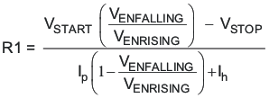
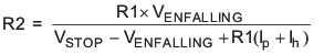
where
- Ih = 3.4 μA
- Ip = 1.15 μA
- VENRISING = 1.21 V
- VENFALLING = 1.17 V