SLVSFN6 December 2020 TPS54622-EP
PRODUCTION DATA
- 1 Features
- 2 Applications
- 3 Description
- 4 Revision History
- 5 Pin Configurations and Functions
- 6 Specifications
-
7 Detailed Description
- 7.1 Overview
- 7.2 Functional Block Diagram
- 7.3
Feature Description
- 7.3.1 Fixed-Frequency PWM Control
- 7.3.2 Continuous Current Mode Operation (CCM)
- 7.3.3 VIN and Power VIN Pins (VIN and PVIN)
- 7.3.4 Voltage Reference
- 7.3.5 Adjusting the Output Voltage
- 7.3.6 Safe Start-Up Into Prebiased Outputs
- 7.3.7 Error Amplifier
- 7.3.8 Slope Compensation
- 7.3.9 Enable and Adjusting Undervoltage Lockout
- 7.3.10 Adjustable Switching Frequency and Synchronization (RT/CLK)
- 7.3.11 Slow Start (SS/TR)
- 7.3.12 Power Good (PWRGD)
- 7.3.13 Output Overvoltage Protection (OVP)
- 7.3.14 Overcurrent Protection
- 7.3.15 Thermal Shutdown
- 7.3.16 Small Signal Model for Loop Response
- 7.3.17 Simple Small Signal Model for Peak Current Mode Control
- 7.3.18 Small Signal Model for Frequency Compensation
- 7.4 Device Functional Modes
-
8 Application and Implementation
- 8.1 Application Information
- 8.2
Typical Application
- 8.2.1 Design Requirements
- 8.2.2
Detailed Design Procedures
- 8.2.2.1 Custom Design With WEBENCH® Tools
- 8.2.2.2 Operating Frequency
- 8.2.2.3 Output Inductor Selection
- 8.2.2.4 Output Capacitor Selection
- 8.2.2.5 Input Capacitor Selection
- 8.2.2.6 Slow-Start Capacitor Selection
- 8.2.2.7 Bootstrap Capacitor Selection
- 8.2.2.8 Undervoltage Lockout Setpoint
- 8.2.2.9 Output Voltage Feedback Resistor Selection
- 8.2.2.10 Compensation Component Selection
- 8.2.2.11 Fast Transient Considerations
- 8.2.3 Application Curves
- 9 Power Supply Recommendations
- 10Layout
- 11Device and Documentation Support
- 12Mechanical, Packaging, and Orderable Information
7.4.4 Sequencing (SS/TR)
Many of the common power supply sequencing methods can be implemented using the SS/TR, EN and PWRGD pins.
The sequential method is illustrated in Figure 7-10 using two TPS54622-EP-EP devices. The power good of the first device is coupled to the EN pin of the second device which enables the second power supply once the primary supply reaches regulation.
 Figure 7-10 Sequential Start-Up Sequence
Figure 7-11 shows the method implementing ratiometric sequencing by connecting the SS/TR pins of two devices together. The regulator outputs ramp up and reach regulation at the same time. When calculating the slow start time the pullup current source must be doubled in Equation 4.
 Figure 7-11 Ratiometric Start-Up Sequence
Ratiometric and simultaneous power supply sequencing can be implemented by connecting the resistor network of R1 and R2 shown in Figure 7-12 to the output of the power supply that needs to be tracked or another voltage reference source. Using Equation 14 and Equation 15, the tracking resistors can be calculated to initiate the Vout2 slightly before, after or at the same time as Vout1. Equation 16 is the voltage difference between Vout1 and Vout2.
To design a ratiometric start-up in which the Vout2 voltage is slightly greater than the Vout1 voltage when Vout2 reaches regulation, use a negative number in Equation 14 and Equation15 for deltaV. Equation 16 results in a positive number for applications where the Vout2 is slightly lower than Vout1 when Vout2 regulation is achieved. .
The deltaV variable is zero volt for simultaneous sequencing. To minimize the effect of the inherent SS/TR to VSENSE offset (Vssoffset, 29 mV) in the slow start circuit and the offset created by the pullup current source (Iss, 2.3 μA) and tracking resistors, the Vssoffset and Iss are included as variables in the equations.
To ensure proper operation of the device, the calculated R1 value from Equation 14 must be greater than the value calculated in Equation 17.
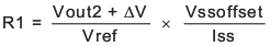
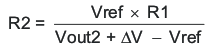
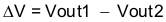
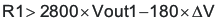
 Figure 7-12 Ratiometric and Simultaneous Start-Up Sequence
There are two final considerations when using a resistor divider to the SS/TR pin for simultaneous start-up. First, as described in Power Good (PWRGD), for the PWRGD output to be active the SS/TR voltage must be above 1.4 V. The external divider may prevent the SS/TR voltage from charging above the threshold. For the SS/TR pin to charge above the threshold, an external MOSFET may be needed to disconnect the resistor divider or modify the resistor divider ratio after start-up is complete. The PWRGD pin of the VOUT(1) converter could be used to turn on or turn off the external MOSFET. Second, a pre-bias on VOUT(1) may prevent VOUT(2) from turning on. When the TPS54622-EP is enabled, an internal 700-Ω MOSFET at the SS/TR pin turns on to discharge the SS/TR voltage as described in Slow Start (SS/TR). The SS/TR pin voltage must discharge below 20 mV before the TPS54622-EP starts up. If the upper resistor at the SS/TR pin is too small, the SS/TR pin does not discharge below the threshold, and VOUT(2) does not ramp up. The upper resistor in the SS/TR divider may need to be increased to allow the SS/TR pin to discharge below the threshold.