SLVSFN6 December 2020 TPS54622-EP
PRODUCTION DATA
- 1 Features
- 2 Applications
- 3 Description
- 4 Revision History
- 5 Pin Configurations and Functions
- 6 Specifications
-
7 Detailed Description
- 7.1 Overview
- 7.2 Functional Block Diagram
- 7.3
Feature Description
- 7.3.1 Fixed-Frequency PWM Control
- 7.3.2 Continuous Current Mode Operation (CCM)
- 7.3.3 VIN and Power VIN Pins (VIN and PVIN)
- 7.3.4 Voltage Reference
- 7.3.5 Adjusting the Output Voltage
- 7.3.6 Safe Start-Up Into Prebiased Outputs
- 7.3.7 Error Amplifier
- 7.3.8 Slope Compensation
- 7.3.9 Enable and Adjusting Undervoltage Lockout
- 7.3.10 Adjustable Switching Frequency and Synchronization (RT/CLK)
- 7.3.11 Slow Start (SS/TR)
- 7.3.12 Power Good (PWRGD)
- 7.3.13 Output Overvoltage Protection (OVP)
- 7.3.14 Overcurrent Protection
- 7.3.15 Thermal Shutdown
- 7.3.16 Small Signal Model for Loop Response
- 7.3.17 Simple Small Signal Model for Peak Current Mode Control
- 7.3.18 Small Signal Model for Frequency Compensation
- 7.4 Device Functional Modes
-
8 Application and Implementation
- 8.1 Application Information
- 8.2
Typical Application
- 8.2.1 Design Requirements
- 8.2.2
Detailed Design Procedures
- 8.2.2.1 Custom Design With WEBENCH® Tools
- 8.2.2.2 Operating Frequency
- 8.2.2.3 Output Inductor Selection
- 8.2.2.4 Output Capacitor Selection
- 8.2.2.5 Input Capacitor Selection
- 8.2.2.6 Slow-Start Capacitor Selection
- 8.2.2.7 Bootstrap Capacitor Selection
- 8.2.2.8 Undervoltage Lockout Setpoint
- 8.2.2.9 Output Voltage Feedback Resistor Selection
- 8.2.2.10 Compensation Component Selection
- 8.2.2.11 Fast Transient Considerations
- 8.2.3 Application Curves
- 9 Power Supply Recommendations
- 10Layout
- 11Device and Documentation Support
- 12Mechanical, Packaging, and Orderable Information
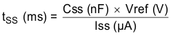
7.3.11 Slow Start (SS/TR)
The device uses the lower voltage of the internal voltage reference or the SS/TR pin voltage as the reference voltage and regulates the output accordingly. A capacitor on the SS/TR pin to ground implements a slow start time. The device has an internal pullup current source of 2.3 μA that charges the external slow-start capacitor. The calculations for the slow start time (tSS, 10% to 90%) and slow-start capacitor (Css) are shown in Equation 4. The voltage reference (Vref) is 0.6 V and the slow start charge current (Iss) is 2.3 μA.
When the input UVLO is triggered, the EN pin is pulled below 1.21 V, or a thermal shutdown event occurs the device stops switching and enters low current operation. At the subsequent power up, when the shutdown condition is removed, the device does not start switching until it has discharged its SS/TR pin to ground ensuring proper soft start behavior.