SLVSC81C September 2013 – February 2016 TPS560200
PRODUCTION DATA.
- 1 Features
- 2 Applications
- 3 Description
- 4 Revision History
- 5 Pin Configuration and Functions
- 6 Specifications
- 7 Detailed Description
- 8 Application and Implementation
- 9 Power Supply Recommendations
- 10Layout
- 11Device and Documentation Support
- 12Mechanical, Packaging, and Orderable Information
10 Layout
10.1 Layout Guidelines
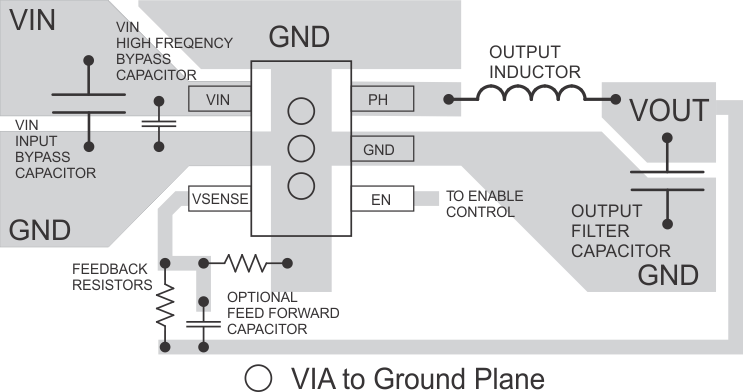
The VIN pin should be bypassed to ground with a low-ESR ceramic bypass capacitor. Take care to minimize the loop area formed by the bypass capacitor connection, the VIN pin, and the GND pin of the IC. The typical recommended bypass capacitance is 10-μF ceramic with a X5R or X7R dielectric and the optimum placement is closest to the VIN and GND pins of the device. An additional high-frequency bypass capacitor may be added. See Figure 19 for a PCB layout example. The GND pin should be tied to the PCB ground plane at the pin of the IC. The PH pin should be routed to a small copper area directly adjacent to the pin. Make the circulating loop from PH to the output inductor, output capacitors and back to GND as tight as possible while preserving adequate etch width to reduce conduction losses in the copper. Connect the exposed thermal pad to bottom or internal layer ground plane using vias as shown. Additional vias may be used adjacent to the IC to tie top-side copper to the internal or bottom layer copper. The additional external components can be placed approximately as shown. It may be possible to obtain acceptable performance with alternate layout schemes; however, this layout produced good results and is intended as a guideline.
10.2 Layout Example
 Figure 19. Layout Schematic