SLVSC81C September   2013  – February 2016 TPS560200

PRODUCTION DATA.  

  1. Features
  2. Applications
  3. Description
  4. Revision History
  5. Pin Configuration and Functions
  6. Specifications
    1. 6.1 Absolute Maximum Ratings
    2. 6.2 ESD Ratings
    3. 6.3 Recommended Operating Conditions
    4. 6.4 Thermal Information
    5. 6.5 Electrical Characteristics
    6. 6.6 Typical Characteristics
  7. Detailed Description
    1. 7.1 Overview
    2. 7.2 Functional Block Diagram
    3. 7.3 Feature Description
      1. 7.3.1 PWM Operation
      2. 7.3.2 PWM Frequency and Adaptive On-Time Control
      3. 7.3.3 Advanced Auto-Skip Eco-Mode Control
      4. 7.3.4 Soft-Start and Prebiased Soft-Start
      5. 7.3.5 Current Protection
      6. 7.3.6 Thermal Shutdown
    4. 7.4 Device Functional Modes
      1. 7.4.1 Normal Operation
      2. 7.4.2 Eco-Mode Operation
      3. 7.4.3 Standby Operation
  8. Application and Implementation
    1. 8.1 Application Information
    2. 8.2 Typical Application
      1. 8.2.1 Design Requirements
      2. 8.2.2 Detailed Design Procedure
        1. 8.2.2.1 Output Voltage Resistors Selection
        2. 8.2.2.2 Output Filter Selection
        3. 8.2.2.3 Input Capacitor Selection
      3. 8.2.3 Application Curves
  9. Power Supply Recommendations
  10. 10Layout
    1. 10.1 Layout Guidelines
    2. 10.2 Layout Example
  11. 11Device and Documentation Support
    1. 11.1 Device Support
      1. 11.1.1 Third-Party Products Disclaimer
    2. 11.2 Trademarks
    3. 11.3 Electrostatic Discharge Caution
    4. 11.4 Glossary
  12. 12Mechanical, Packaging, and Orderable Information

パッケージ・オプション

メカニカル・データ(パッケージ|ピン)
サーマルパッド・メカニカル・データ
発注情報

5 Pin Configuration and Functions

DBV Package
5-Pin SOT-23
(Top View)
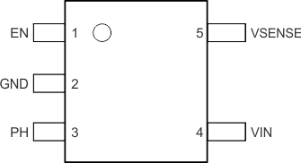
TPS560200 pin_assignmts_SLVSC81.gif

Pin Functions

PIN I/O DESCRIPTION
NAME NO.
EN 1 I Enable pin. Float to enable
GND 2 Return for control circuitry and low-side power MOSFET
PH 3 O The switch node
VIN 4 I Supplies the control circuitry of the power converter
VSENSE 5 I Converter feedback input. Connect to output voltage with feedback resistor divider