SLVSC81C September 2013 – February 2016 TPS560200
PRODUCTION DATA.
- 1 Features
- 2 Applications
- 3 Description
- 4 Revision History
- 5 Pin Configuration and Functions
- 6 Specifications
- 7 Detailed Description
- 8 Application and Implementation
- 9 Power Supply Recommendations
- 10Layout
- 11Device and Documentation Support
- 12Mechanical, Packaging, and Orderable Information
6 Specifications
6.1 Absolute Maximum Ratings(1)
| MIN | MAX | UNIT | ||
|---|---|---|---|---|
| Input voltage | VIN | –0.3 | 20 | V |
| EN | –0.3 | 7 | ||
| VSENSE | –0.3 | 3 | ||
| Output voltage | PH | –0.6 | 20 | |
| PH 10-ns transient | –2 | 20 | ||
| Source current | EN | ±100 | µA | |
| PH | Current limit | A | ||
| Sink current | PH | Current limit | A | |
| Operating junction temperature | –40 | 125 | °C | |
| Storage temperature, Tstg | –65 | 150 | ||
(1) Stresses beyond those listed under Absolute Maximum Ratings may cause permanent damage to the device. These are stress ratings only, and functional operation of the device at these or any other conditions beyond those indicated under Recommended Operating Conditions is not implied. Exposure to absolute-maximum-rated conditions for extended periods may affect device reliability.
6.2 ESD Ratings
| VALUE | UNIT | |||
|---|---|---|---|---|
| V(ESD) | Electrostatic discharge | Human-body model (HBM), per ANSI/ESDA/JEDEC JS-001(1) | ±2000 | V |
| Charged-device model (CDM), per JEDEC specification JESD22-C101(2) | ±500 | |||
(1) JEDEC document JEP155 states that 500-V HBM allows safe manufacturing with a standard ESD control process.
(2) JEDEC document JEP157 states that 250-V CDM allows safe manufacturing with a standard ESD control process.
6.3 Recommended Operating Conditions
over operating free-air temperature range (unless otherwise noted)| MIN | MAX | UNIT | ||
|---|---|---|---|---|
| VI | Input voltage range | 4.5 | 17 | V |
| TJ | Operating junction temperature | –40 | 125 | °C |
6.4 Thermal Information
| THERMAL METRIC(1) | TPS560200 | UNIT | |
|---|---|---|---|
| DBV | |||
| 5 Pins | |||
| RθJA | Junction-to-ambient thermal resistance | 166.8 | °C/W |
| RθJC(top) | Junction-to-case (top) thermal resistance | 100 | |
| RθJB | Junction-to-board thermal resistance | 75.5 | |
| ψJT | Junction-to-top characterization parameter | 29.2 | |
| ψJB | Junction-to-board characterization parameter | 3.7 | |
| RθJC(bot) | Junction-to-case (bottom) thermal resistance | 28.7 | |
(1) For more information about traditional and new thermal metrics, see the Semiconductor and IC Package Thermal Metrics application report, SPRA953.
6.5 Electrical Characteristics
TJ = –40°C to 125°C, VIN = 4.5 V to 17 V (unless otherwise noted)| PARAMETER | TEST CONDITIONS | MIN | TYP | MAX | UNIT |
|---|---|---|---|---|---|
| SUPPLY VOLTAGE (VIN PIN) | |||||
| VIN Operating input voltage | 4.5 | 17 | V | ||
| VIN Internal UVLO threshold | VIN Rising | 3.9 | 4.35 | 4.5 | V |
| VIN Internal UVLO hysteresis | 200 | mV | |||
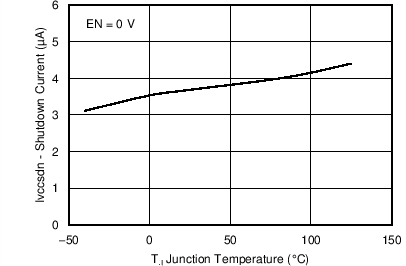
| VIN Shutdown supply current | EN = 0 V, VIN = 12 V | 2.0 | 3.7 | 9 | µA |
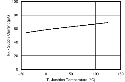
| VIN Operating– non switching supply current | VSENSE = 850 mV, VIN = 12 V | 35 | 60 | 95 | µA |
| ENABLE (EN PIN) | |||||
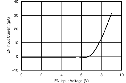
| Enable threshold | Rising | 1.16 | 1.29 | V | |
| Falling | 1.05 | 1.13 | V | ||
| Internal Soft-Start | VSENSE ramps from 0 V to 0.8 V | 2 | ms | ||
| OUTPUT VOLTAGE | |||||
| Voltage reference | 25°C, VIN = 12 V, VOUT = 1.05 V, IOUT = 5 mA, Pulse-Skipping | 0.796 | 0.804 | 0.812 | V |
| 25°C, VIN = 12 V, VOUT = 1.05 V, IOUT = 100 mA, Continuous current mode | 0.792 | 0.800 | 0.808 | V | |
| VIN = 12 V, VOUT = 1.05 V, IOUT = 100 mA, Continuous current mode | 0.789 | 0.800 | 0.811 | V | |
| MOSFET | |||||
| High-side switch resistance(2)(1) | VIN = 12 V | 0.50 | 0.95 | 1.50 | Ω |
| Low-side switch resistance(2) | VIN = 12 V | 0.20 | 0.33 | 0.55 | Ω |
| CURRENT LIMIT | |||||
| Low-side switch sourcing current limit | LOUT = 10 µH, Valley current, VOUT = 1.05 V | 550 | 650 | 775 | mA |
| THERMAL SHUTDOWN | |||||
| Thermal shutdown | 170 | °C | |||
| Thermal shutdown hysteresis | 10 | °C | |||
| ON-TIME TIMER CONTROL | |||||
| On time | VIN = 12 V | 130 | 165 | 200 | ns |
| Minimum off time | 25°C, VSENSE = 0.5 V | 250 | 400 | ns | |
| OUTPUT UNDERVOLTAGE PROTECTION | |||||
| Output UVP threshold | Falling | 56 | 63 | 69 | %VREF |
| Hiccup time | 15 | ms | |||
(1) Measured at pins
(2) Not production tested
6.6 Typical Characteristics
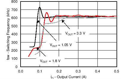
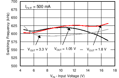
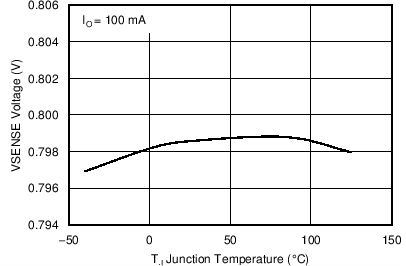
VIN = 12 V, TA = 25°C (unless otherwise noted).