JAJSGB2D May   2015  – August 2021 TPS61088

PRODUCTION DATA  

  1. 特長
  2. アプリケーション
  3. 概要
  4. Revision History
  5. Pin Configuration and Functions
  6. Specifications
    1. 6.1 Absolute Maximum Ratings
    2. 6.2 ESD Ratings
    3. 6.3 Recommended Operating Conditions
    4. 6.4 Thermal Information
    5. 6.5 Electrical Characteristics
    6. 6.6 Typical Characteristics
  7. Detailed Description
    1. 7.1 Overview
    2. 7.2 Functional Block Diagram
    3. 7.3 Feature Description
      1. 7.3.1 Enable and Start-up
      2. 7.3.2 Undervoltage Lockout (UVLO)
      3. 7.3.3 Adjustable Switching Frequency
      4. 7.3.4 Adjustable Peak Current Limit
      5. 7.3.5 Overvoltage Protection
      6. 7.3.6 Thermal Shutdown
    4. 7.4 Device Functional Modes
      1. 7.4.1 Operation
        1. 7.4.1.1 PWM Mode
        2. 7.4.1.2 PFM Mode
  8. Application and Implementation
    1. 8.1 Application Information
    2. 8.2 Typical Application
      1. 8.2.1 Design Requirements
      2. 8.2.2 Detailed Design Procedure
        1. 8.2.2.1 Custom Design with WEBENCH Tools
        2. 8.2.2.2 Setting Switching Frequency
        3. 8.2.2.3 Setting Peak Current Limit
        4. 8.2.2.4 Setting Output Voltage
        5. 8.2.2.5 Inductor Selection
        6. 8.2.2.6 Input Capacitor Selection
        7. 8.2.2.7 Output Capacitor Selection
        8. 8.2.2.8 Loop Stability
      3. 8.2.3 Application Curves
  9. Power Supply Recommendations
  10. 10Layout
    1. 10.1 Layout Guidelines
    2. 10.2 Layout Example
    3. 10.3 Thermal Considerations
  11. 11Device and Documentation Support
    1. 11.1 Device Support
      1. 11.1.1 Third-Party Products Disclaimer
      2. 11.1.2 Development Support
        1. 11.1.2.1 Custom Design with WEBENCH Tools
    2. 11.2 Receiving Notification of Documentation Updates
    3. 11.3 サポート・リソース
    4. 11.4 Trademarks
    5. 11.5 Electrostatic Discharge Caution
    6. 11.6 Glossary
  12. 12Mechanical, Packaging, and Orderable Information

パッケージ・オプション

メカニカル・データ(パッケージ|ピン)
サーマルパッド・メカニカル・データ
発注情報

Adjustable Peak Current Limit

To avoid an accidental large peak current, an internal cycle-by-cycle current limit is adopted. The low-side switch is turned off immediately as soon as the switch current touches the limit. The peak switch current limit can be set by a resistor at the ILIM pin to ground. The relationship between the current limit and the resistance depends on the status of the MODE pin.

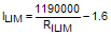
When the MODE pin is floating, namely the TPS61088, is set to work in the PFM mode at light load, use Equation 3 to calculate the resistor value:

Equation 3. GUID-EF4529EC-0445-418C-8CE5-A59BADA9CA09-low.gif

where

  • RILIM is the resistance between the ILIM pin and ground
  • ILIM is the switch peak current limit

When the resistor value is 100 kΩ, the typical current limit is 11.9 A.

When the MODE pin is connected to ground, namely the TPS61088 is set to work in forced PWM mode at light load, use Equation 4 to calculate the resistor value.

Equation 4. GUID-AEF98738-E856-4302-8F14-62F69E66E261-low.gif

When the resistor value is 100 kΩ, the typical current limit is 10.3 A.

Considering the device variation and the tolerance over temperature, the minimum current limit at the worst case can be 1.3 A lower than the value calculated by above equations.