JAJSGB2D May   2015  – August 2021 TPS61088

PRODUCTION DATA  

  1. 特長
  2. アプリケーション
  3. 概要
  4. Revision History
  5. Pin Configuration and Functions
  6. Specifications
    1. 6.1 Absolute Maximum Ratings
    2. 6.2 ESD Ratings
    3. 6.3 Recommended Operating Conditions
    4. 6.4 Thermal Information
    5. 6.5 Electrical Characteristics
    6. 6.6 Typical Characteristics
  7. Detailed Description
    1. 7.1 Overview
    2. 7.2 Functional Block Diagram
    3. 7.3 Feature Description
      1. 7.3.1 Enable and Start-up
      2. 7.3.2 Undervoltage Lockout (UVLO)
      3. 7.3.3 Adjustable Switching Frequency
      4. 7.3.4 Adjustable Peak Current Limit
      5. 7.3.5 Overvoltage Protection
      6. 7.3.6 Thermal Shutdown
    4. 7.4 Device Functional Modes
      1. 7.4.1 Operation
        1. 7.4.1.1 PWM Mode
        2. 7.4.1.2 PFM Mode
  8. Application and Implementation
    1. 8.1 Application Information
    2. 8.2 Typical Application
      1. 8.2.1 Design Requirements
      2. 8.2.2 Detailed Design Procedure
        1. 8.2.2.1 Custom Design with WEBENCH Tools
        2. 8.2.2.2 Setting Switching Frequency
        3. 8.2.2.3 Setting Peak Current Limit
        4. 8.2.2.4 Setting Output Voltage
        5. 8.2.2.5 Inductor Selection
        6. 8.2.2.6 Input Capacitor Selection
        7. 8.2.2.7 Output Capacitor Selection
        8. 8.2.2.8 Loop Stability
      3. 8.2.3 Application Curves
  9. Power Supply Recommendations
  10. 10Layout
    1. 10.1 Layout Guidelines
    2. 10.2 Layout Example
    3. 10.3 Thermal Considerations
  11. 11Device and Documentation Support
    1. 11.1 Device Support
      1. 11.1.1 Third-Party Products Disclaimer
      2. 11.1.2 Development Support
        1. 11.1.2.1 Custom Design with WEBENCH Tools
    2. 11.2 Receiving Notification of Documentation Updates
    3. 11.3 サポート・リソース
    4. 11.4 Trademarks
    5. 11.5 Electrostatic Discharge Caution
    6. 11.6 Glossary
  12. 12Mechanical, Packaging, and Orderable Information

パッケージ・オプション

メカニカル・データ(パッケージ|ピン)
サーマルパッド・メカニカル・データ
発注情報

Thermal Considerations

The maximum IC junction temperature should be restricted to 125°C under normal operating conditions. Calculate the maximum allowable dissipation, PD(max), and keep the actual power dissipation less than or equal to PD(max). The maximum-power-dissipation limit is determined using Equation 21.
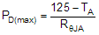
Equation 21. GUID-2E845CF0-B8C3-494E-A5CB-E5B3FFC360DC-low.gif

where

  • TA is the maximum ambient temperature for the application.
  • RθJA is the junction-to-ambient thermal resistance given in the Thermal Information table.

The TPS61088 comes in a thermally-enhanced VQFN package. This package includes a thermal pad that improves the thermal capabilities of the package. The real junction-to-ambient thermal resistance of the package greatly depends on the PCB type, layout, and thermal pad connection. Using thick PCB copper and soldering the thermal pad to a large ground plate enhance the thermal performance. Using more vias connects the ground plate on the top layer and bottom layer around the IC without solder mask also improves the thermal capability.