JAJSGJ5E November 2014 – February 2021 TPS65218
PRODUCTION DATA
- 1 特長
- 2 アプリケーション
- 3 概要
- 4 Revision History
- 5 Pin Configuration and Functions
- 6 Specifications
-
7 Detailed Description
- 7.1 Overview
- 7.2 Functional Block Diagram
- 7.3
Feature Description
- 7.3.1
Wake-Up and Power-Up and Power-Down Sequencing
- 7.3.1.1 Power-Up Sequencing
- 7.3.1.2 Power-Down Sequencing
- 7.3.1.3 Strobe 1 and Strobe 2
- 7.3.1.4 Supply Voltage Supervisor and Power-Good (PGOOD)
- 7.3.1.5 Backup Supply Power-Good (PGOOD_BU)
- 7.3.1.6 Internal LDO (INT_LDO)
- 7.3.1.7 Current Limited Load Switches
- 7.3.1.8 LDO1
- 7.3.1.9 Coin Cell Battery Voltage Acquisition
- 7.3.1.10 UVLO
- 7.3.1.11 Power-Fail Comparator
- 7.3.1.12 Battery-Backup Supply Power-Path
- 7.3.1.13 DCDC3 and DCDC4 Power-Up Default Selection
- 7.3.1.14 I/O Configuration
- 7.3.1.15 Push Button Input (PB)
- 7.3.1.16 AC_DET Input (AC_DET)
- 7.3.1.17 Interrupt Pin (INT)
- 7.3.1.18 I2C Bus Operation
- 7.3.1
Wake-Up and Power-Up and Power-Down Sequencing
- 7.4 Device Functional Modes
- 7.5 Register Maps
- 8 Application and Implementation
- 9 Power Supply Recommendations
- 10Layout
- 11Device and Documentation Support
- 12Mechanical, Packaging, and Orderable Information
パッケージ・オプション
メカニカル・データ(パッケージ|ピン)
サーマルパッド・メカニカル・データ
発注情報
7.3.1.14.1 Configuring GPO2 as Open-Drain Output
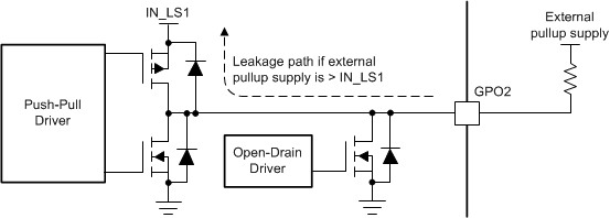
GPO2 may be configured as open-drain or push-pull output. The supply for the push-pull driver is internally connected to the IN_LS1 input pin, whereas an external pull-up resistor and supply are required in the open-drain configuration. Because of the internal connection to IN_LS1, the external pull-up supply must not exceed the voltage on the IN_LS1 pin, otherwise leakage current may be observed from GPO2 to IN_LS1 as shown in Figure 7-22.
 Figure 7-22 GPO2 as Open-Drain Output
Note:
When configured as open-drain output, the external pull-up supply must not exceed the voltage level on IN_LS1 pin.