JAJSHS4B August 2019 – December 2019 TPS66020 , TPS66021
PRODUCTION DATA.
- 1 特長
- 2 アプリケーション
- 3 概要
- 4 改訂履歴
- 5 Pin Configuration and Functions
-
6 Specifications
- 6.1 Absolute Maximum Ratings
- 6.2 ESD Ratings
- 6.3 Recommended Operating Conditions
- 6.4 Recommended Supply Load Capacitance
- 6.5 Thermal Information
- 6.6 PP5V Power Switch Characteristics
- 6.7 PPHV Power Switch Characteristics
- 6.8 Power Path Supervisory
- 6.9 VBUS LDO Characteristics
- 6.10 Thermal Shutdown Characteristics
- 6.11 Input-output (I/O) Characteristics
- 6.12 Power Consumption Characteristics
- 6.13 Typical Characteristics
- 7 Parameter Measurement Information
-
8 Detailed Description
- 8.1 Overview
- 8.2 Functional Block Diagram
- 8.3 Feature Description
- 8.4 Device Functional Modes
-
9 Application and Implementation
- 9.1 Application Information
- 9.2
Typical Application
- 9.2.1 Design Requirements
- 9.2.2
Detailed Design Procedure
- 9.2.2.1 External Current Reference Resistor (RIREF)
- 9.2.2.2 External VLDO Capacitor (CVLDO)
- 9.2.2.3 PP5V Power Path Capacitance
- 9.2.2.4 PPHV, VBUS Power Path Capacitance
- 9.2.2.5 VBUS TVS Protection (Optional)
- 9.2.2.6 VBUS Schottky Diode Protection (Optional)
- 9.2.2.7 VBUS Overvoltage Protection (Optional)
- 9.2.2.8 Dead Battery Support
- 9.2.2.9 Fast Role Swap (FRS) (Optional)
- 9.2.3 Application Curves
- 10Power Supply Recommendations
- 11Layout
- 12デバイスおよびドキュメントのサポート
- 13メカニカル、パッケージ、および注文情報
8.3.4 VBUS Overvoltage Protection (OVP)
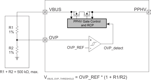
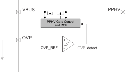
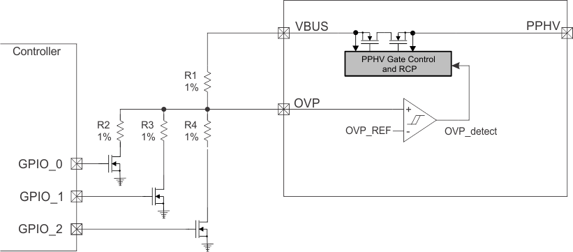
TPS6602x supports overvoltage protection on the VBUS terminal. When the voltage detected on OVP exceeds a set level, the PPHV power path will automatically be disabled (if enabled), and will remain disabled until the OVP event is removed. FLT is asserted when an overvoltage event occurs. The VBUS OVP threshold may be set using a resistor divider from VBUS to GND, whose divider output is connected to the OVP terminal as shown in Figure 11. Table 1 shows resistor divider settings for common USB Power Delivery fixed voltage supply contracts along with the resulting nominal OVP thresholds. These thresholds may be adjusted based on desired margins for a given application. If VBUS OVP is not required or needs to be disabled, the OVP terminal may be tied or driven to GND as shown in Figure 12. Lastly, as one example implementation, the OVP threshold may be controlled dynamically using outputs from a PD controller or microcontroller as shown in Figure 13. By selecting each output, different VBUS OVP threshold settings are possible.
 Figure 11. VBUS OVP Threshold Set by External Resistor Divider
 Table 1. Typical External Resistor Divider Settings
| PD Fixed Contract | R1, kΩ | R2, kΩ | Nominal VBUS OVP Threshold, V |
|---|---|---|---|
| 5 V | 102 | 20 | 6.1 |
| 9 V | 182 | 20 | 10.1 |
| 15 V | 309 | 20 | 16.5 |
| 20 V | 432 | 20 | 22.6 |
 Figure 12. VBUS OVP Disabled
  Figure 13. Selectable VBUS OVP Thresholds