JAJSHS4B August 2019 – December 2019 TPS66020 , TPS66021
PRODUCTION DATA.
- 1 特長
- 2 アプリケーション
- 3 概要
- 4 改訂履歴
- 5 Pin Configuration and Functions
-
6 Specifications
- 6.1 Absolute Maximum Ratings
- 6.2 ESD Ratings
- 6.3 Recommended Operating Conditions
- 6.4 Recommended Supply Load Capacitance
- 6.5 Thermal Information
- 6.6 PP5V Power Switch Characteristics
- 6.7 PPHV Power Switch Characteristics
- 6.8 Power Path Supervisory
- 6.9 VBUS LDO Characteristics
- 6.10 Thermal Shutdown Characteristics
- 6.11 Input-output (I/O) Characteristics
- 6.12 Power Consumption Characteristics
- 6.13 Typical Characteristics
- 7 Parameter Measurement Information
-
8 Detailed Description
- 8.1 Overview
- 8.2 Functional Block Diagram
- 8.3 Feature Description
- 8.4 Device Functional Modes
-
9 Application and Implementation
- 9.1 Application Information
- 9.2
Typical Application
- 9.2.1 Design Requirements
- 9.2.2
Detailed Design Procedure
- 9.2.2.1 External Current Reference Resistor (RIREF)
- 9.2.2.2 External VLDO Capacitor (CVLDO)
- 9.2.2.3 PP5V Power Path Capacitance
- 9.2.2.4 PPHV, VBUS Power Path Capacitance
- 9.2.2.5 VBUS TVS Protection (Optional)
- 9.2.2.6 VBUS Schottky Diode Protection (Optional)
- 9.2.2.7 VBUS Overvoltage Protection (Optional)
- 9.2.2.8 Dead Battery Support
- 9.2.2.9 Fast Role Swap (FRS) (Optional)
- 9.2.3 Application Curves
- 10Power Supply Recommendations
- 11Layout
- 12デバイスおよびドキュメントのサポート
- 13メカニカル、パッケージ、および注文情報
9.2.3 Application Curves
1.
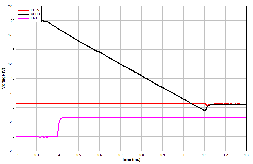
Figure 32. Fast Role Swap Response, 20-V Sink Contract, CVBUS= 20 µF, IVBUS = 0.5 A 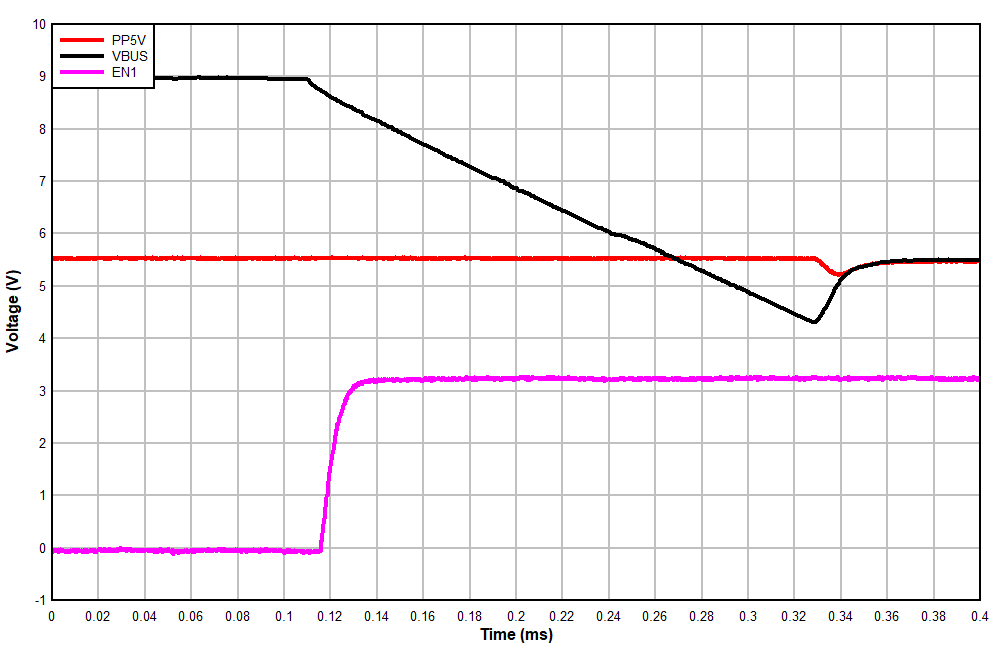
1.
Figure 34. Fast Role Swap Response, 9-V Sink Contract, CVBUS= 20 µF, IVBUS = 0.5 A 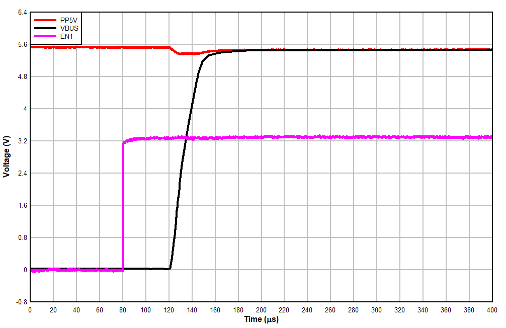
1.
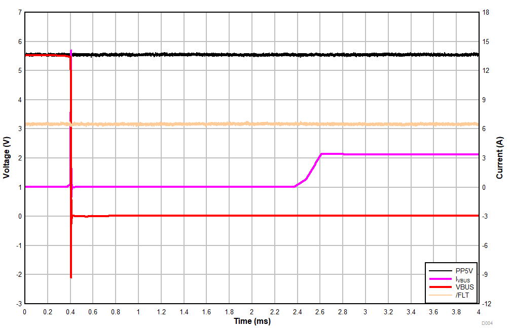
Figure 36. Fast Role Swap Response, 5-V Sink Contract, VBUS Fully Discharged, CVBUS= 20 µF, IVBUS = 0.5 A 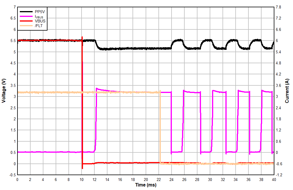 Figure 31. PP5V Enable into Short with Thermal Cycling
1.
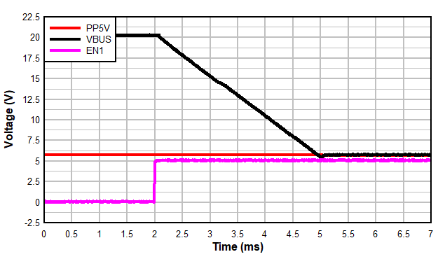
Figure 33. Fast Role Swap Response, 20-V Sink Contract, CVBUS= 120 µF, IVBUS = 0.5 A 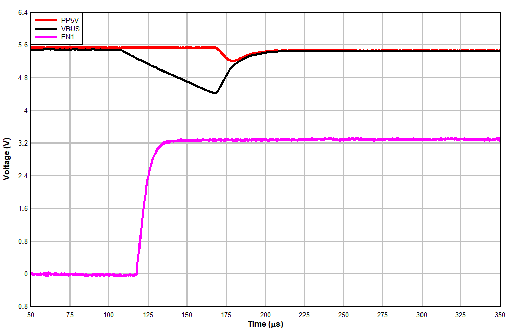
1.
Figure 35. Fast Role Swap Response, 5-V Sink Contract, CVBUS= 20 µF, IVBUS = 0.5 A 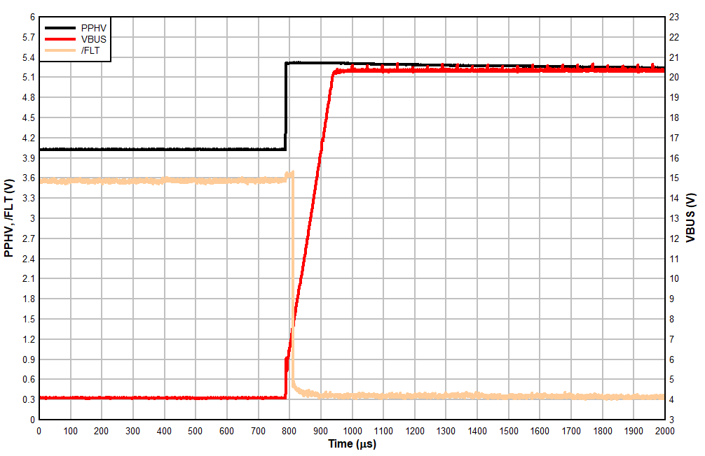
1.
Figure 37. VBUS OVP Response with 6-V Threshold 