JAJS012J October 2004 – November 2018 TPS75003
PRODUCTION DATA.
- 1 特長
- 2 アプリケーション
- 3 概要
- 4 改訂履歴
- 5 Pin Configuration and Functions
- 6 Specifications
-
7 Detailed Description
- 7.1 Overview
- 7.2 Functional Block Diagram
- 7.3
Feature Description
- 7.3.1 Operation (Buck Controllers)
- 7.3.2 Enable (Buck Controllers)
- 7.3.3 UVLO (Buck Controllers)
- 7.3.4 Current Limit (Buck Controllers)
- 7.3.5 Short-Circuit Protection (Buck Controllers)
- 7.3.6 Soft-Start (Buck Controllers)
- 7.3.7 LDO Operation
- 7.3.8 Internal Current Limit (LDO)
- 7.3.9 Enable Pin (LDO)
- 7.3.10 Dropout Voltage (LDO)
- 7.3.11 Transient Response (LDO)
- 7.3.12 Thermal Protection (LDO)
- 7.3.13 Power Dissipation (LDO)
-
8 Application and Implementation
- 8.1 Application Information
- 8.2
Typical Application
- 8.2.1 Design Requirements
- 8.2.2
Detailed Design Procedure
- 8.2.2.1 Input Capacitor CIN1, CIN2 Selection (Buck Controllers)
- 8.2.2.2 Inductor Value Selection (Buck Controllers)
- 8.2.2.3 External PMOS Transistor Selection (Buck Controllers)
- 8.2.2.4 Diode Selection (Buck Controllers)
- 8.2.2.5 Output Capacitor Selection (Buck Controllers)
- 8.2.2.6 Output Voltage Ripple Effect on VOUT (Buck Controllers)
- 8.2.2.7 Soft-Start Capacitor Selection (Buck Controllers)
- 8.2.2.8 Output Voltage Setting Selection (Buck Controllers)
- 8.2.2.9 Input Capacitor Selection (LDO)
- 8.2.2.10 Output Capacitor Selection (LDO)
- 8.2.2.11 Soft-Start Capacitor Selection (LDO)
- 8.2.2.12 Setting Output Voltage (LDO)
- 8.2.3 Application Curves
- 9 Power Supply Recommendations
- 10Layout
- 11デバイスおよびドキュメントのサポート
- 12メカニカル、パッケージ、および注文情報
パッケージ・オプション
メカニカル・データ(パッケージ|ピン)
- RHL|20
サーマルパッド・メカニカル・データ
- RHL|20
発注情報
7.3.1 Operation (Buck Controllers)
Channels 1 and 2 have two identical non-synchronous buck controllers that use minimum on-time and minimum off-time hysteretic control (see Figure 18. For clarity, BUCK1 is used throughout the discussion of device operation. When VOUT1 is less than its target, an external PMOS (Q1) is turned on for at least the minimum on-time, increasing current through the inductor (L1) until VOUT1 reaches its target value or the current limit (set by R1) is reached. When either of these conditions is met, the PMOS is switched off for at least the minimum off-time of the device. After the minimum off-time has passed, the output voltage is monitored and the switch is turned on again when necessary.
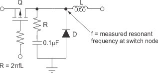
When output current is low, the buck controllers operate in discontinuous mode. In this mode, each switching cycle begins at zero inductor current, rises to a maximum value, then falls back to zero current. When current reaches zero on the falling edge, ringing occurs at the resonant frequency of the inductor and stray switch node capacitance. This operation is normal; it does not affect circuit performance, and can be minimized if desired by using an RC snubber, a resistor in series with the gate of the PMOS, or both as shown in Figure 15.
 Figure 15. RC Snubber and Series Gate Resistor Used to Minimize Ringing
 At higher output currents, the TPS75003 device operates in continuous mode. In continuous mode, there is no ringing at the switch node and VOUT is equal to VIN times the duty cycle of the switching waveform.
When VIN approaches or falls to less than VOUT, the buck controllers operate in 100% duty cycle mode, fully turning on the external PMOS to let regulation occur at a lower dropout than would otherwise be possible.