JAJS012J October 2004 – November 2018 TPS75003
PRODUCTION DATA.
- 1 特長
- 2 アプリケーション
- 3 概要
- 4 改訂履歴
- 5 Pin Configuration and Functions
- 6 Specifications
-
7 Detailed Description
- 7.1 Overview
- 7.2 Functional Block Diagram
- 7.3
Feature Description
- 7.3.1 Operation (Buck Controllers)
- 7.3.2 Enable (Buck Controllers)
- 7.3.3 UVLO (Buck Controllers)
- 7.3.4 Current Limit (Buck Controllers)
- 7.3.5 Short-Circuit Protection (Buck Controllers)
- 7.3.6 Soft-Start (Buck Controllers)
- 7.3.7 LDO Operation
- 7.3.8 Internal Current Limit (LDO)
- 7.3.9 Enable Pin (LDO)
- 7.3.10 Dropout Voltage (LDO)
- 7.3.11 Transient Response (LDO)
- 7.3.12 Thermal Protection (LDO)
- 7.3.13 Power Dissipation (LDO)
-
8 Application and Implementation
- 8.1 Application Information
- 8.2
Typical Application
- 8.2.1 Design Requirements
- 8.2.2
Detailed Design Procedure
- 8.2.2.1 Input Capacitor CIN1, CIN2 Selection (Buck Controllers)
- 8.2.2.2 Inductor Value Selection (Buck Controllers)
- 8.2.2.3 External PMOS Transistor Selection (Buck Controllers)
- 8.2.2.4 Diode Selection (Buck Controllers)
- 8.2.2.5 Output Capacitor Selection (Buck Controllers)
- 8.2.2.6 Output Voltage Ripple Effect on VOUT (Buck Controllers)
- 8.2.2.7 Soft-Start Capacitor Selection (Buck Controllers)
- 8.2.2.8 Output Voltage Setting Selection (Buck Controllers)
- 8.2.2.9 Input Capacitor Selection (LDO)
- 8.2.2.10 Output Capacitor Selection (LDO)
- 8.2.2.11 Soft-Start Capacitor Selection (LDO)
- 8.2.2.12 Setting Output Voltage (LDO)
- 8.2.3 Application Curves
- 9 Power Supply Recommendations
- 10Layout
- 11デバイスおよびドキュメントのサポート
- 12メカニカル、パッケージ、および注文情報
パッケージ・オプション
メカニカル・データ(パッケージ|ピン)
- RHL|20
サーマルパッド・メカニカル・データ
- RHL|20
発注情報
7.3.4 Current Limit (Buck Controllers)
An external resistor (R1 or R2) is used to set the current limit for the external PMOS transistor (Q1 or Q2). These resistors are connected between IN1 and IS1 (or IN2 and IS2) to provide a reference voltage across these pins that is proportional to the current flowing through the PMOS transistor. This reference voltage is compared to an internal reference to determine if an overcurrent condition exists. When current limit is exceeded, the external PMOS is turned off for the minimum off-time. Current limit detection is disabled for 10ns any time the PMOS is turned on to avoid triggering on switching noise. In 100% duty cycle mode, current limit is always enabled. Current limit is calculated using the VIS1 or VIS2 specification in the Electrical Characteristics section as shown in Equation 1.

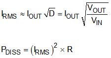
The current limit resistor must be appropriately rated for the dissipated power determined by its RMS current calculated by Equation 2.

For low-cost applications the IS1,2 pin can be connected to the drain of the PMOS, using RDS,ON instead of R1 or R2 to set current limit. Variations in the PMOS RDS,ON must be considered to make sure that current limit will protect external components such as the inductor, the diode, and the switch itself from damage as a result of overcurrent.