JAJSBN7C SEPTEMBER 2011 – April 2018 TPS84210
PRODUCTION DATA.
- 1 特長
- 2 アプリケーション
- 3 概要
- 4 改訂履歴
- 5 Pin Configuration and Functions
- 6 Specifications
- 7 Functional Block Diagram
- 8 Application and Implementation
- 9 Capacitor Recommendations For The TPS84210 Power Supply
- 10Transient Response
- 11Application Schematics
- 12Power Good (PWRGD)
- 13Power-Up Characteristics
- 14Remote Sense
- 15Output On/Off Inhibit (INH)
- 16Slow Start (SS/TR)
- 17Overcurrent Protection
- 18Synchronization (CLK)
- 19Sequencing (SS/TR)
- 20Programmable Undervoltage Lockout (UVLO)
- 21Thermal Shutdown
- 22Layout Guidelines
- 23Layout Example
- 24EMI
- 25デバイスおよびドキュメントのサポート
- 26メカニカル、パッケージ、および注文情報
パッケージ・オプション
メカニカル・データ(パッケージ|ピン)
- RKG|39
サーマルパッド・メカニカル・データ
- RKG|39
発注情報
6.7 Typical Characteristics (VIN = 3.3 V)
The electrical characteristic data has been developed from actual products tested at 25°C. This data is considered typical for the converter. Applies to Figure 6, Figure 7, and Figure 8. The temperature derating curves represent the conditions at which internal components are at or below the manufacturer's maximum operating temperatures. Derating limits apply to devices soldered directly to a 100 mm × 100 mm double-sided PCB with 1 oz. copper. Applies to Figure 9. Figure 6. Efficiency vs. Output Current
 Figure 8. Power Dissipation vs. Output Current
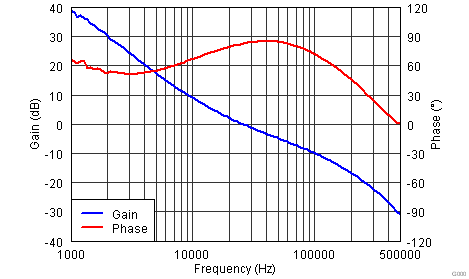
 Figure 10. VOUT= 1.8 V, IOUT= 2 A, COUT1= 47 µF ceramic, COUT2= 100 µF POSCAP, fSW= 1 MHz
 Figure 7. Voltage Ripple vs. Output Current
 Figure 9. Safe Operating Area