JAJSF89C March 2013 – December 2019 TPS84A20
PRODUCTION DATA.
- 1 特長
- 2 アプリケーション
- 3 概要
- 4 改訂履歴
- 5 概要(続き)
- 6 Ordering Information
- 7 Specifications
- 8 Device Information
- 9 Typical Characteristics (PVIN = VIN = 12 V)
- 10Typical Characteristics (PVIN = VIN = 5 V)
- 11Typical Characteristics (PVIN = 3.3 V, VIN = 5 V)
-
12Application Information
- 12.1 Adjusting the Output Voltage
- 12.2 Capacitor Recommendations for the TPS84A20 Power Supply
- 12.3 Transient Response
- 12.4 Transient Waveforms
- 12.5 Application Schematics
- 12.6 VIN and PVIN Input Voltage
- 12.7 3.3 V PVIN Operation
- 12.8 Power Good (PWRGD)
- 12.9 Light Load Efficiency (LLE)
- 12.10 SYNC_OUT
- 12.11 Parallel Operation
- 12.12 Power-Up Characteristics
- 12.13 Pre-Biased Start-Up
- 12.14 Remote Sense
- 12.15 Thermal Shutdown
- 12.16 Output On/Off Inhibit (INH)
- 12.17 Slow Start (SS/TR)
- 12.18 Overcurrent Protection
- 12.19 Synchronization (CLK)
- 12.20 Sequencing (SS/TR)
- 12.21 Programmable Undervoltage Lockout (UVLO)
- 12.22 Layout Considerations
- 12.23 EMI
- 13デバイスおよびドキュメントのサポート
- 14メカニカル、パッケージ、および注文情報
パッケージ・オプション
デバイスごとのパッケージ図は、PDF版データシートをご参照ください。
メカニカル・データ(パッケージ|ピン)
- RVQ|42
サーマルパッド・メカニカル・データ
発注情報
12.16 Output On/Off Inhibit (INH)
The INH pin provides electrical on/off control of the device. Once the INH pin voltage exceeds the threshold voltage, the device starts operation. If the INH pin voltage is pulled below the threshold voltage, the regulator stops switching and enters low quiescent current state.
The INH pin has an internal pullup current source, allowing the user to float the INH pin for enabling the device. If an application requires controlling the INH pin, use an open drain/collector device, or a suitable logic gate to interface with the pin.
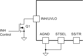
Figure 29 shows the typical application of the inhibit function. The Inhibit control has its own internal pullup to VIN potential. An open-collector or open-drain device is recommended to control this input.
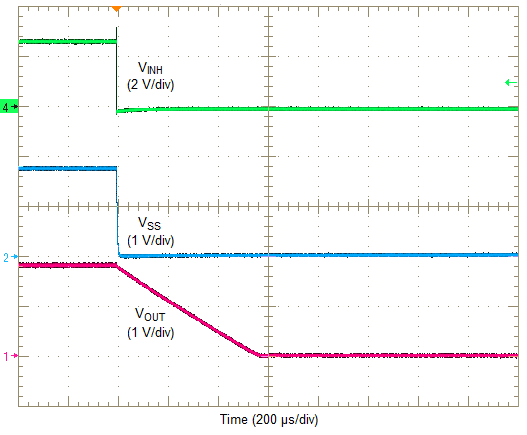
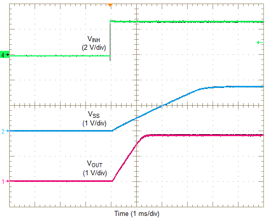
Turning Q1 on applies a low voltage to the inhibit control (INH) pin and disables the output of the supply, shown in Figure 30. If Q1 is turned off, the supply executes a soft-start power-up sequence, as shown in Figure 31. A regulated output voltage is produced within 2 ms. The waveforms were measured with a 5-A constant current load.
 Figure 29. Typical Inhibit Control
  Figure 30. Inhibit Turn-Off
  Figure 31. Inhibit Turn-On