JAJSHS0C March 2019 – March 2021 TPS92682-Q1
PRODUCTION DATA
- 1 特長
- 2 アプリケーション
- 3 概要
- 4 Revision History
- 5 Pin Configuration and Functions
- 6 Specifications
-
7 Detailed Description
- 7.1 Overview
- 7.2 Functional Block Diagram
- 7.3
Feature Description
- 7.3.1 Device Enable
- 7.3.2 Internal Regulator and Undervoltage Lockout (UVLO)
- 7.3.3 Oscillator
- 7.3.4 Spread Spectrum Function
- 7.3.5 Gate Driver
- 7.3.6 Rail-to-Rail Current Sense Amplifier
- 7.3.7 Transconductance Error Amplifier
- 7.3.8 Switch Current Sense
- 7.3.9 Slope Compensation
- 7.3.10 ILED Setting in CC Mode
- 7.3.11 Output Voltage Setting in CV Mode
- 7.3.12 PWM Dimming
- 7.3.13 P-Channel FET Gate Driver Output
- 7.3.14 Soft Start
- 7.3.15 Two-Phase Operation
- 7.3.16 Faults and Diagnostics
- 7.4 Device Functional Modes
- 7.5 Programming
- 7.6
TPS92682 Registers
- 7.6.1 EN Register
- 7.6.2 CFG1 Register
- 7.6.3 CFG2 Register
- 7.6.4 SWDIV Register
- 7.6.5 ISLOPE Register
- 7.6.6 FM Register
- 7.6.7 SOFTSTART Register
- 7.6.8 CH1IADJ Register
- 7.6.9 CH2IADJ Register
- 7.6.10 PWMDIV Register
- 7.6.11 CH1PWML Register
- 7.6.12 CH1PWMH Register
- 7.6.13 CH2PWML Register
- 7.6.14 CH2PWMH Register
- 7.6.15 ILIM Register
- 7.6.16 IFT Register
- 7.6.17 MFT Register
- 7.6.18 FLT1 Register (read only)
- 7.6.19 FLT2 Register (read only)
- 7.6.20 FEN1 Register
- 7.6.21 FEN2 Register
- 7.6.22 FLATEN Register
- 7.6.23 OV Register
- 7.6.24 LHCFG Register
- 7.6.25 LHCH1IADJ Register
- 7.6.26 LHCH2IADJ Register
- 7.6.27 LHCH1PWML Register
- 7.6.28 LHCH1PWMH Register
- 7.6.29 LHCH2PWML Register
- 7.6.30 LHCH2PWMH Register
- 7.6.31 LHILIM Register
- 7.6.32 LHIFT Register
- 7.6.33 LHMFT Register
- 7.6.34 LHFEN1 Register
- 7.6.35 LHFEN2 Register
- 7.6.36 LHFLATEN Register
- 7.6.37 LHOV Register
- 7.6.38 CAL Register
- 7.6.39 RESET Register
-
8 Application and Implementation
- 8.1 Application Information General Design Considerations
- 8.2 Application Information CC Mode
- 8.3 Typical Application CV Mode
- 8.4
Typical Application CC Mode
- 8.4.1 CC Boost Design Requirements
- 8.4.2
CC Boost Detailed Design Procedure
- 8.4.2.1 Calculating Duty Cycle
- 8.4.2.2 Setting Switching Frequency
- 8.4.2.3 Setting Dither Modulation Frequency
- 8.4.2.4 Inductor Selection
- 8.4.2.5 Output Capacitor Selection
- 8.4.2.6 Input Capacitor Selection
- 8.4.2.7 Main N-Channel MOSFET Selection
- 8.4.2.8 Rectifier Diode Selection
- 8.4.2.9 Setting ILED and Selecting RCS
- 8.4.2.10 Setting Switch Current Limit
- 8.4.2.11 Slope Compensation
- 8.4.2.12 Compensator Parameters
- 8.4.2.13 Overvoltage Protection
- 8.4.2.14 Series P-Channel MOSFET Selection
- 8.4.3 CC Buck-Boost Design Requirements
- 8.4.4
CC Buck-Boost Detailed Design Procedure
- 8.4.4.1 Calculating Duty Cycle
- 8.4.4.2 Setting Switching Frequency
- 8.4.4.3 Setting Dither Modulation Frequency
- 8.4.4.4 Inductor Selection
- 8.4.4.5 Output Capacitor Selection
- 8.4.4.6 Input Capacitor Selection
- 8.4.4.7 Main N-Channel MOSFET Selection
- 8.4.4.8 Rectifier Diode Selection
- 8.4.4.9 Setting ILED and Selecting RCS
- 8.4.4.10 Setting Switch Current Limit
- 8.4.4.11 Slope Compensation
- 8.4.4.12 Compensator Parameters
- 8.4.4.13 Overvoltage Protection
- 8.4.5 PWM Dimming Consideration
- 8.4.6 Application Curves
- 8.5
Typical Application CV Mode
- 8.5.1 CV Design Requirements
- 8.5.2
Detailed Design Procedure
- 8.5.2.1 Calculating Duty Cycle
- 8.5.2.2 Setting Switching Frequency
- 8.5.2.3 Setting Dither Modulation Frequency
- 8.5.2.4 Inductor Selection
- 8.5.2.5 Output Capacitor Selection
- 8.5.2.6 Input Capacitor Selection
- 8.5.2.7 Main N-Channel MOSFET Selection
- 8.5.2.8 Rectifier Diode Selection
- 8.5.2.9 Programming VOUT
- 8.5.2.10 Setting Switch Current Limit
- 8.5.2.11 Slope Compensation
- 8.5.2.12 Compensator Parameters
- 8.5.2.13 Overvoltage Protection
- 8.5.3 Application Curves
- 9 Power Supply Recommendations
- 10Layout
- 11Device and Documentation Support
- 12Mechanical, Packaging, and Orderable Information
パッケージ・オプション
メカニカル・データ(パッケージ|ピン)
サーマルパッド・メカニカル・データ
発注情報
7.3.12 PWM Dimming
As shown in Figure 7-10, the TPS92682-Q1 device incorporates both internal and external PWM dimming. To select between external or internal PWM dimming, the INTPWM bit in CFG1 Register must be set to "0" or "1", respectively. If internal PWM dimming operation is selected, the state of the PWMx pins do not have any effect on the operation of the device. For external PWM dimming, apply a square-wave signal to the PWMx pin with the rising and falling thresholds provided in the Electrical Characteristics. The LED current modulates based on the duty cycle of the external PWM signal, DPWM(EXT).
 Figure 7-10 PWM Dimming Circuit
To use internal PWM dimming, the INTPWM bit in CFG1 Register must be set to "1". The TPS92682-Q1 device incorporates a 10-bit PWM counter for each channel. The duty cycle of the internal PWM can be set using a 10-bit value in the CHxPWML and CHxPWMH registers. Because CHxPWM is a 10-bit value, a PWM duty cycle update can require two SPI writes, one to the CHxPWMH and another to the CHxPWML register. To prevent transferring incoherent values, the contents of the two registers transfer to the CHxPWM counter only upon the write to the CHxPWML register. Therefore, for an update to the PWM duty cycle, it is recommended consecutively writing to CHxPWMH first and CHxPWML second. In addition, in order to avoid corrupting the progress of the current PWM duty cycle, the update from the CHxPWM registers to the CHxPWM counter occurs two PWMCLK before the end of each PWM period (at the count of 1022).
Due to synchronization of the external PWM with internal clock, when switching from external PWM to internal PWM, a glitch for the total of one PWM period can be observed in the output.
The clock to the 10-bit PWM counter is related to the main clock, CLKM, by a division factor set by a 3-bit value in the PWMDIV Register. The relation between the PWMCLK and PWM frequency with CLKM frequency are shown in Equation 3 and Equation 4.
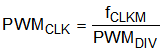
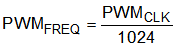
For example, if the CLKM frequency is set to fCLKM = 800 kHz and PWMDIV = 001 (division value of 2), the PWM frequency is PWMFREQ ≈ 390 Hz.
The phase between the internal PWM dimming for the two channels can be set to 180° if the PWMPH bit in CFG1 Register is set to 0. For PWMPH = 1, there is zero phase shift between the internal 10-bit PWM counters of the two channels.
The PWM signal controls the GATEx and PDRVx outputs. If PWMxINT is set low, the associated channel is turned off, the COMPx pin is disconnected from the error amplifier, and the PDRVx output is set to VCSP to maintain the charge on the compensation network and output capacitors. On the rising edge of the PWMxINT, the GATEx and PDRVx outputs are enabled to ramp the inductor current to the previous steady-state value. The COMPx pin connects to the error amplifier only when the switch current sense voltage VISPx exceeds the COMPx voltage, CHx_comp. This connection immediately forces the converter into steady-state operation with minimum LED current overshoot. When dimming is not required, connect the PWMx pins to the VDD pin. An internal pull-down resistor sets the PWM inputs to logic-low and disables the device when the pins are disconnected or left floating, and the INTPWM bit in CFG1 Register is set to the default value of "0".