JAJS127E April 1999 – August 2016 UCC2813-0 , UCC2813-1 , UCC2813-2 , UCC2813-3 , UCC2813-4 , UCC2813-5 , UCC3813-0 , UCC3813-1 , UCC3813-2 , UCC3813-3 , UCC3813-4 , UCC3813-5
PRODUCTION DATA.
- 1 特長
- 2 アプリケーション
- 3 概要
- 4 改訂履歴
- 5 Device Comparison Table
- 6 Pin Configuration and Functions
- 7 Specifications
-
8 Detailed Description
- 8.1 Overview
- 8.2 Functional Block Diagram
- 8.3
Feature Description
- 8.3.1 Detailed Pin Descriptions
- 8.3.2 Undervoltage Lockout (UVLO)
- 8.3.3 Self-Biasing, Active Low Output
- 8.3.4 Reference Voltage
- 8.3.5 Oscillator
- 8.3.6 Synchronization
- 8.3.7 PWM Generator
- 8.3.8 Minimum Off-Time Adjustment (Dead-Time Control)
- 8.3.9 Leading Edge Blanking
- 8.3.10 Minimum Pulse Width
- 8.3.11 Current Limiting
- 8.3.12 Overcurrent Protection and Full-Cycle Restart
- 8.3.13 Soft Start
- 8.3.14 Slope Compensation
- 8.4 Device Functional Modes
-
9 Application and Implementation
- 9.1 Application Information
- 9.2
Typical Application
- 9.2.1 Design Requirements
- 9.2.2
Detailed Design Procedure
- 9.2.2.1 Bulk Capacitor Calculation
- 9.2.2.2 Transformer Design
- 9.2.2.3 MOSFET and Output Diode Selection
- 9.2.2.4 Output Capacitor Calculation
- 9.2.2.5 Current Sensing Network
- 9.2.2.6 Gate Drive Resistor
- 9.2.2.7 REF Bypass Capacitor
- 9.2.2.8 RT and CT
- 9.2.2.9 Start-Up Circuit
- 9.2.2.10 Voltage Feedback Compensation Procedure
- 9.2.3 Application Curves
- 10Power Supply Recommendations
- 11Layout
- 12デバイスおよびドキュメントのサポート
- 13メカニカル、パッケージ、および注文情報
パッケージ・オプション
デバイスごとのパッケージ図は、PDF版データシートをご参照ください。
メカニカル・データ(パッケージ|ピン)
- D|8
- PW|8
サーマルパッド・メカニカル・データ
発注情報
10 Power Supply Recommendations
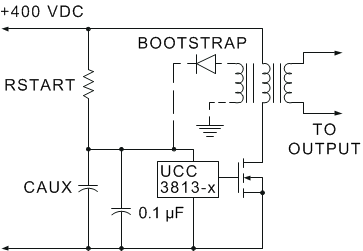
An internal VCC shunt regulator is incorporated into each member of the UCCx813-x family to limit the supply voltage to approximately 13.5 V. A series resistor from VCC to the input supply source is required with inputs above 12 V to limit the shunt regulator current. A maximum of 10 mA can be shunted to ground by the internal regulator. The internal regulator in conjunction with the device’s low start-up and operating current can greatly simplify powering the device and may eliminate the requirement for a regulated bootstrap auxiliary supply and winding in many applications. The supply voltage is MOSFET gate level compatible and requires no external Zener diode or regulator protection with a current-limited input supply. The UVLO start-up threshold is 1 V below the shunt regulator level on the UCCx813-[2,4] devices to ensure start-up. It is important to bypass the device's supply (VCC) and reference voltage (REF) pins each with a 0.1-µF to 1-µF ceramic capacitor to ground. The capacitors must be placed as close to the actual pin connections as possible for optimal noise filtering. A second, larger filter capacitor may also be required in offline applications to hold the supply voltage (VVCC) above the UVLO turnoff threshold during start-up.
 Figure 43. Different Ways to Power Up the Device