JAJS127E April 1999 – August 2016 UCC2813-0 , UCC2813-1 , UCC2813-2 , UCC2813-3 , UCC2813-4 , UCC2813-5 , UCC3813-0 , UCC3813-1 , UCC3813-2 , UCC3813-3 , UCC3813-4 , UCC3813-5
PRODUCTION DATA.
- 1 特長
- 2 アプリケーション
- 3 概要
- 4 改訂履歴
- 5 Device Comparison Table
- 6 Pin Configuration and Functions
- 7 Specifications
-
8 Detailed Description
- 8.1 Overview
- 8.2 Functional Block Diagram
- 8.3
Feature Description
- 8.3.1 Detailed Pin Descriptions
- 8.3.2 Undervoltage Lockout (UVLO)
- 8.3.3 Self-Biasing, Active Low Output
- 8.3.4 Reference Voltage
- 8.3.5 Oscillator
- 8.3.6 Synchronization
- 8.3.7 PWM Generator
- 8.3.8 Minimum Off-Time Adjustment (Dead-Time Control)
- 8.3.9 Leading Edge Blanking
- 8.3.10 Minimum Pulse Width
- 8.3.11 Current Limiting
- 8.3.12 Overcurrent Protection and Full-Cycle Restart
- 8.3.13 Soft Start
- 8.3.14 Slope Compensation
- 8.4 Device Functional Modes
-
9 Application and Implementation
- 9.1 Application Information
- 9.2
Typical Application
- 9.2.1 Design Requirements
- 9.2.2
Detailed Design Procedure
- 9.2.2.1 Bulk Capacitor Calculation
- 9.2.2.2 Transformer Design
- 9.2.2.3 MOSFET and Output Diode Selection
- 9.2.2.4 Output Capacitor Calculation
- 9.2.2.5 Current Sensing Network
- 9.2.2.6 Gate Drive Resistor
- 9.2.2.7 REF Bypass Capacitor
- 9.2.2.8 RT and CT
- 9.2.2.9 Start-Up Circuit
- 9.2.2.10 Voltage Feedback Compensation Procedure
- 9.2.3 Application Curves
- 10Power Supply Recommendations
- 11Layout
- 12デバイスおよびドキュメントのサポート
- 13メカニカル、パッケージ、および注文情報
パッケージ・オプション
デバイスごとのパッケージ図は、PDF版データシートをご参照ください。
メカニカル・データ(パッケージ|ピン)
- D|8
- PW|8
サーマルパッド・メカニカル・データ
発注情報
8 Detailed Description
8.1 Overview
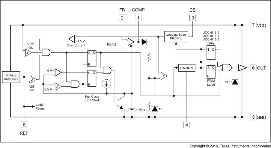
The UCCx813-x family of high-speed, low-power integrated circuits contain all of the control and drive functions required for off-line and DC-to-DC fixed-frequency current-mode switched-mode power supplies having minimal external parts count. The UCCx813-x family is a cost-reduced version of the UCCx80x family, with some relaxation of certain parameter limits. See Differences Between the UCC3813 and UCC3800 PWM Families for more information.
These devices have the same pin configuration as the UCx84x and UCx84xA families, and also offer the added features of internal full-cycle soft start and internal leading-edge blanking of the current-sense input. The UCCx813-x devices are pin-out compatible with the UCx84x and UCx84xA families, however they are not plug-in compatible. In general, the UCCx813-x requires fewer external components and consumes less operating current.
8.2 Functional Block Diagram
8.3 Feature Description
The UCCx813-x family offers numerous advantages that allow the power supply design engineer to meet their challenging requirements.
Features include:
- Bi-CMOS process
- Low starting supply current: typically 100 µA
- Low operating supply current: typically 500 µA
- Pinout compatible with UC3842 and UC3842A families
- 5-V operation (UCCx813-[3,5])
- Leading-edge blanking of current-sense signal
- On-chip soft start for start-up and fault recovery
- Internal full cycle restart delay
- 1.5% voltage reference
- Up to 1-MHz oscillator
- Low self-biasing output during UVLO
- 70-ns response from current sense to output
- Very few external components required
- Available in surface-mount and PDIP packages
8.3.1 Detailed Pin Descriptions
8.3.1.1 COMP
COMP is the output of the error amplifier and the input of the PWM comparator. Unlike earlier-generation devices, the error amplifier in the UCCx813-x device family is a true low-output-impedance 2-MHz operational amplifier. As such, the COMP terminal both sources and sinks current. However, the error amplifier is internally current limited, so zero duty cycle may be commanded by externally forcing COMP to GND.
The UCCx813-x device family features built-in full cycle soft start at power up and after fault recovery, and no external components are necessary. Soft start is implemented as a rising clamp on the COMP voltage, increasing from 0 V to 5 V in 4 ms.
8.3.1.2 CS
CS is the input to the current-sense comparators. The UCCx813-x current sense is significantly different from its predecessor. The UCCx813-x device family has two different current-sense comparators: the PWM comparator and an overcurrent comparator. The overcurrent comparator is intended only for fault sensing, and exceeding the overcurrent threshold causes a soft-start cycle. The earlier UC3842 family current-sense input connects to only the PWM comparator.
The UCCx813-x device family contains digital current-sense filtering, which disconnects the CS terminal from the current sense comparator during the 100-ns interval immediately following the rising edge of the OUT pin. This digital filtering, also called leading-edge blanking, prevents false triggering due to leading edge noises which means that in most applications, no analog filtering (external R-C filter) is required on CS. Compared to an external RC filter technique, the leading-edge blanking provides a smaller effective CS-to-OUT delay. However, the minimum non-zero on-time of the OUT signal is determined by the leading-edge-blanking time and the CS-to-OUT propagation delay. The gain of the current sense amplifier is typically 1.65 V/V in the UCCx813-x family versus typically 3 V/V in the UC3842 family. Connect CS directly to MOSFET source current sense resistor.
8.3.1.3 FB
FB is the inverting input of the error amplifier. For best stability, keep the FB lead length as short as possible and FB stray capacitance as small as possible. At 2 MHz, the gain-bandwidth of the error amplifier is twice that of earlier UC3842 family devices, and feedback design techniques are identical.
8.3.1.4 GND
GND is the signal reference ground and power ground for all functions on this part. TI recommends separating the signal return paths and the high current gate driver path so that signals are not affected by the switching current.
8.3.1.5 OUT
OUT is the output of a high-current power driver capable of driving the gate of a power MOSFET with peak currents exceeding ±750 mA (up to ±1 A). OUT is actively held low when VCC is below the UVLO threshold. This feature eliminates the need for a gate-to-source bleeder resistor associated with the MOSFET gate drive.
The high-current power driver consists of CMOS FET output devices, which can switch all of the way to GND and all of the way to VCC. The output provides very smooth rising and falling waveforms, providing very low impedances to overshoot and undershoot which means that in many cases, external Schottky clamp diodes may not be necessary on the output. Finally, no external gate voltage clamp is necessary with the UCCx813-x as the on-chip Zener diode automatically clamps the output to VCC.
8.3.1.6 RC
RC is the oscillator timing pin. For fixed frequency operation, set the timing-capacitor charging current by connecting a resistor from REF to RC. Set frequency by connecting a timing capacitor from RC to GND. For best performance, keep the timing capacitor lead to GND as short and direct as possible. If possible, use separate ground traces for the timing capacitor and all other functions.
The UCCx813-x’s oscillator allows for operation to 1 MHz versus 500 kHz with the UC3842 family. Both devices make use of an external resistor to set the charging current for the capacitor, which determines the oscillator frequency. For the UCCx813-[0,1,2,4], use Equation 1.

where
- ƒ is the oscillator frequency in hertz (Hz)
- R is the timining resistance in ohms (Ω)
- C is the timing capacitance in farads (F)
For the UCCx813-[3,5], use Equation 2.

The recommended timing resistance is from 10 kΩ to 200 kΩ and timing capacitance is from 100 pF to 1000 pF. Never use a timing resistor less than 10 kΩ.
The two equations are different due to different reference voltages. The peak-to-peak amplitude of the oscillator waveform is 2.45 V versus 1.7 V in UC3842 family. For best performance, keep the timing capacitor lead to GND as short as possible. TI recommends separate ground traces for the timing capacitor and all other pins. The maximum duty cycle for the UCCx813-[0,2,3] is approximately 99%; the maximum duty cycle for the UCCx813-[1,4,5] is approximately 49%. The duty cycle cannot be easily modified by adjusting RT and CT, unlike the UC3842A family. The maximum duty cycle limit is set by the ratio of the external oscillator charging resistor RT and the internal oscillator discharge transistor on-resistance, like the UC3842. However, maximum duty cycle limits less than 90% (for the UCCx813-[0,2,3]) and less than 45% (for the UCCx813-[1,4,5]) can not reliably be set in this manner. For better control of maximum duty cycle, consider using the UCCx807.
8.3.1.7 REF
REF is the voltage reference for the error amplifier and also for many other functions on the IC. REF is also used as the logic power supply for high speed switching logic on the IC. The UCCx813-[0,1,2,4] have a 5-V reference and the UCCx813-[3,5] have a 4-V reference. Both have ±1.5% accuracy at 25°C versus ±2% in the UC3842 family. The REF output short-circuit current is lower at 5 mA, compared to 30 mA in the UC3842 family.
For reference stability and to prevent noise problems with high speed switching transients, it is important to bypass REF to GND with a ceramic capacitor as close to the pins as possible. A minimum of 0.1-µF ceramic is required. Additional REF bypassing is required for external loads greater than 2.5 mA on the reference. An electrolytic capacitor can also be used in addition to the ceramic capacitor.
When VCC is greater than 1 V and less than the UVLO on-threshold, REF is internally pulled to ground through a 5-kΩ resistor which means that REF can be used as a logic output indicating power-system status.
8.3.1.8 VCC
VCC is the power input connection for this device. In normal operation, VCC is powered through a current limiting resistor to a low-impedance source. To prevent noise problems, bypass VCC to GND with a 0.1-µF ceramic capacitor in parallel as close to the VCC pin as possible. An electrolytic capacitor can also be used in addition to the ceramic capacitor.
Although quiescent VCC current is very low, total supply current is higher, depending on the OUT current. Total VCC current is the sum of quiescent VCC current and the average OUT current. Knowing the switching frequency f and the MOSFET gate charge (Qg), average OUT current can be calculated from Equation 3.

The UCCx813-x has a lower VCC (supply voltage) clamp of 13.5 V typical versus 30 V on the UC3842. For applications that require a higher VCC voltage, a resistor must be placed in series with VCC to increase the source impedance. The maximum value of this resistor is calculated with Equation 4.

where
- VIN(min) is the minimum voltage that is used to supply VCC
- VVCC(max) is the maximum VCC clamp voltage of the controller
- IVCC is the IC supply current without considering the gate driver current
- Qg is the external power MOSFET gate charge, and f is the switching frequency
Additionally, the UCCx813-x has an on-chip Zener diode to limit VCC to 13.5 V, which also limits the maximum OUT voltage. If the bias-supply source is always lower than 12 V, it may be connected directly to VCC. With UVLO thresholds at 4.1 V and 3.6 V for the UCCx813-3 and UCCx813-5, respectively, 5-V PWM operation is now possible.
8.3.2 Undervoltage Lockout (UVLO)
The UCCx813-x devices feature undervoltage lockout protection circuits for controlled operation during power-up and power-down sequences. Both the supply voltage (VVCC) and the reference voltage (VREF) are monitored by the UVLO circuitry. During UVLO, an active-low, self-biasing totem-pole output structure is also incorporated for enhanced power switch protection.
Undervoltage lockout thresholds for the UCCx813-[2,3,4,5] devices are different from the previous generation of UCx84[2,3,4,5] PWM controllers. The thresholds are optimized for two groups of applications: off-line power supplies and DC-DC converters. See Table 1 for the specific thresholds for each device.
Table 1. UVLO Level Comparison Table
| DEVICE | VON (V) | VOFF (V) |
|---|---|---|
| UCCx813-0 | 7.2 | 6.9 |
| UCCx813-1 | 9.4 | 7.4 |
| UCCx813-[2,4] | 12.5 | 8.3 |
| UCCx813-[3,5] | 4.1 | 3.6 |
The UCCx813-[2,4] feature typical UVLO thresholds of 12.5 V for turnon and 8.3 V for turnoff, providing 4.3 V of hysteresis.
For low voltage inputs, which include battery and 5-V applications, the UCCx813-[3,5] turn on at 4.1 V and turn off at 3.6 V with 0.5 V of hysteresis.
The UCCx813-[0,1] have UVLO thresholds optimized for automotive and battery applications.
During UVLO, the device draws approximately 100 µA of supply current. Once VCC crosses the turnon threshold, the IC supply current increases typically to about 500 µA, over an order of magnitude lower than bipolar counterparts. Figure 11 indicates the supply current behavior at the relative UVLO turnon and turnoff thresholds, not including average OUT current.
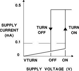 Figure 11. IC Supply Current at UVLO
8.3.3 Self-Biasing, Active Low Output
The self-biasing, active-low clamp circuit shown in Figure 12 eliminates the potential for problematic MOSFET turnon. As the PWM output voltage rises while in UVLO, the P-channel device drives the larger N-channel switch ON, which clamps the output voltage low. Power to this circuit is supplied by the externally rising gate voltage, so full protection is available regardless of the device's supply voltage during undervoltage lockout.
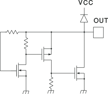 Figure 12. Internal Circuit Holding OUT Low During UVLO
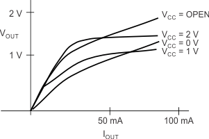 Figure 13. OUT Voltage vs OUT Current During UVLO
8.3.4 Reference Voltage
The traditional 5-V band-gap-derived reference voltage of the UC3842 family can be also found on the UCCx813-[0,1,2,4] devices. However, the reference voltage of the UCCx813-[3,5] devices is 4 V. This change was necessary to facilitate operation with input supply voltages below 5 V. Many of the reference voltage specifications are similar to the UC3842 devices although the test conditions have been changed, indicative of lower-current PWM applications. Similar to their bipolar counterparts, the BiCMOS devices internally pull the reference voltage low during UVLO, which can be used as a logic status indication.
The 4-V reference voltage on the UCCx813-[3,5] is derived from the supply voltage (VVCC) and requires about 0.5 V of headroom to maintain regulation. Whenever VVCC is below approximately 4.5 V, the reference voltage also drops outside of its specified range for normal operation. The relationship between VVCC and VREF during this excursion is shown in Figure 14.
The noninverting input to the error amplifier is tied to one-half of the controller's reference voltage (VREF). This input is 2 V on the UCCx813-[3,5] and 2.5 V on the higher reference voltage parts: the UCCx813-[0,1,2,4].
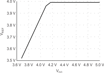 Figure 14. UCC3813-3 REF Output vs VVCC
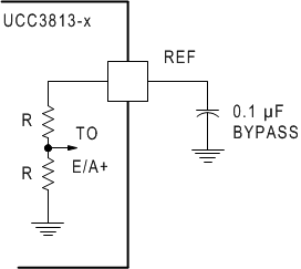 Figure 15. Required Reference Bypass Minimum Capacitance
8.3.5 Oscillator
The UCCx813-x oscillator generates a sawtooth waveform on RC. The rise time is set by the time constant of RT and CT. The fall time is set by CT and an internal transistor on-resistance of approximately 130 Ω. During the fall time, the output is OFF and the maximum duty cycle is reduced below 50% or 100%, depending on the part number. Larger values for the timing capacitor increase the discharge time and reduce the maximum duty cycle and frequency slightly, as seen in Figure 5 and Figure 6 .
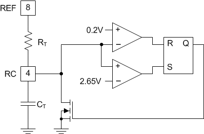 Figure 16. Oscillator Equivalent Circuit
The oscillator section of the UCCx813-x BiCMOS family has few similarities to the UC3842 type — other than single-pin programming. It does still use a resistor to the reference voltage and capacitor to ground to program the oscillator frequency up to 1 MHz. Timing component values must be changed because a much lower charging current is desirable for low-power operation. Several characteristics of the oscillator have been optimized for high-speed, noise-immune operation. The oscillator peak-to-peak amplitude has been increased to 2.45 V typical versus 1.7 V on the UC3842 family. The lower oscillator threshold has been dropped to approximately 0.2 V while the upper threshold remains fairly close to the original 2.8 V at approximately 2.65 V.
Discharge current of the timing capacitor has been increased to nearly 20-mA peak as opposed to roughly 8 mA. This can be represented by approximately 130 Ω in series with the discharge switch to ground. The higher current is necessary to achieve brief dead times and high duty cycles with high-frequency operation. Practical applications can use these devices to a 1-MHz switching frequency.
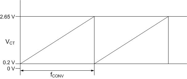 Figure 17. Oscillator Waveform at RC
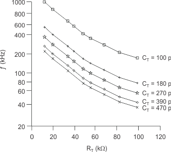 Figure 18. Oscillator Frequency vs RT For Several CT
8.3.6 Synchronization
Synchronization of these PWM controllers is best obtained by the universal technique shown in Figure 19. The device oscillator is programmed to free-run at a frequency about 20% lower than that of the synchronizing frequency. A brief positive pulse is applied across the 50-Ω resistor to force synchronization. Typically, a 1-V amplitude pulse of 100-ns width is sufficient for most applications.
The controller can also be synchronized to a pulse-train applied directly to the oscillator RC pin. The device internally pulls low at this node once the upper oscillator threshold is crossed. This 130-Ω impedance to ground remains active until the voltage on RC is lowered below 0.2 V. External synchronization circuits must accommodate these conditions.
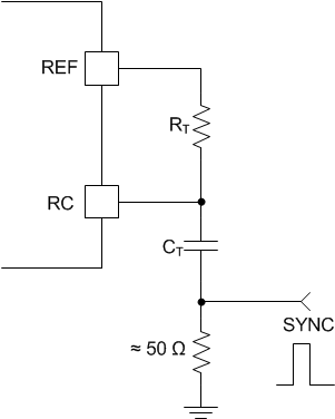 Figure 19. Synchronizing the Oscillator
8.3.7 PWM Generator
Maximum duty cycle is higher for these devices than for their UC384[2,3,4,5] predecessors. This is primarily due to the higher ratio of timing capacitor discharge-to-charge current, which can exceed one hundred-to-one in a typical BiCMOS application. Attempts to program the oscillator maximum duty cycle much below the specified range, by adjusting the timing component values of RT and CT, must be avoided. There are two reasons to refrain from this design practice. First, the device's high discharge current would necessitate higher charging current than necessary for programming, defeating the purpose of low power operation. Second, a low-value timing resistor may prevent the capacitor from discharging to the lower threshold and initiating the next switching cycle.
8.3.8 Minimum Off-Time Adjustment (Dead-Time Control)
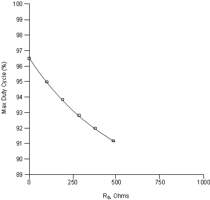
Dead time is the term used to describe the ensured OFF time of the PWM output during each oscillator cycle. It is used to ensure that even at maximum duty cycle, there is enough time to reset the magnetic circuit elements, and prevent saturation. The dead time of the UCCx813-x PWM family is determined by the internal 130-Ω discharge impedance and the timing capacitor value. Larger capacitance values extend the dead time whereas smaller values results in higher maximum duty cycles for the same operating frequency. A curve for dead time versus timing capacitor values is provided in Figure 20. Further increasing the dead time is possible by adding a low-value resistor between the RC pin and the timing components, as shown in Figure 21. The dead time increases with increasing discharge resistor value to about 470 Ω as indicated from the curve in Figure 22. Higher resistances must be avoided as they can decrease the dead time and reduce the oscillator peak-to-peak amplitude. Sinking too much current (1 mA) by reducing RT will freeze the oscillator OFF by preventing discharge to the lower comparator threshold voltage of 0.2 V. Adding this discharge control resistor has several impacts on the oscillator programming. First, it introduces a DC offset to the capacitor during the discharge interval – but not the charging interval of the timing cycle, thus lowering the usable peak-to-peak timing capacitor amplitude. Because of the reduced peak-to-peak amplitude, the exact value of CT may require adjustment to obtain the correct oscillator frequency. One alternative is keep the same value timing capacitor and adjust both the timing and discharge resistor values because these are readily available in finer numerical increments.
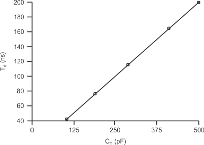 Figure 20. Minimum Dead Time vs CT
| RT = 20 kΩ |
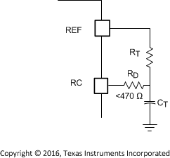 Figure 21. Circuit to Produce Controlled Maximum Duty Cycle
8.3.9 Leading Edge Blanking
A 100-ns leading-edge-blanking interval is applied to the current-sense input circuitry of the UCCx813-x devices. This internal feature eliminates the requirement for an external resistor-capacitor filter network to suppress the switching spike associated with turnon of the power MOSFET. This 100-ns period should be adequate for most switch-mode designs but can be lengthened by adding an external R/C filter. The 100-ns leading edge blanking is also applied to the overcurrent fault comparator in addition to the cycle-by-cycle current-limiting PWM function.
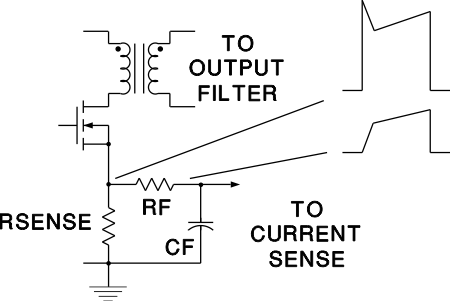 Figure 23. Current-Sense Filter Required
With Older PWM Devices
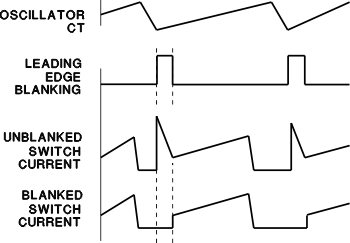 Figure 24. UCCx813-x Current-Sense Waveforms
With Leading Edge Blanking
8.3.10 Minimum Pulse Width
The PWM comparator has two inputs; one is from the current sense input, the other input is the attenuated error-amplifier output (COMP) that has a diode and two resistors in series to ground. The diode in this network is used to ensure that zero duty-cycle can be reached. Whenever the E/A output falls below a diode forward voltage drop, no current flows in the resistor divider and the PWM input goes to zero, resulting in zero pulse width.
Under certain conditions, the leading-edge-blanking circuitry can lead to an output pulse of minimum width equal to the blanking interval. This occurs when the COMP is slightly higher than a diode forward voltage drop of about 0.5 V, such that the attenuated COMP input to the PWM comparator allows an output pulse to start. If the attenuated COMP level commands a peak current whose pulse width would fall within the leading-edge-blanking interval, the output will remain ON until the blanking interval is finished and the peak current will be higher than desired by the COMP level. The usual result is that the converter output voltage rises, increasing the error, and COMP is driven lower than the diode drop which then produces zero pulse width. Cycle-skipping may result as the output voltage rises and falls around this minimum pulse-width condition.
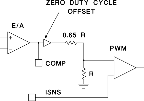 Figure 25. Zero Duty-Cycle Offset
8.3.11 Current Limiting
A 1-V (typical) cycle-by-cycle current limit threshold is incorporated into the UCCx813-x family. The 100-ns leading-edge-blanking interval is applied to this current-limiting circuitry. The blanking overrides the current-limit comparator output to prevent the leading-edge switch noise from triggering a current-limit function. Propagation delay from the current-limit comparator to the output is typically 70 ns. This high-speed path minimizes power semiconductor dissipation during an overload by abbreviating the ON time.
For increased efficiency in the current-sense circuitry, the circuit shown in Figure 26 can be used. Resistors RA and RB bias the actual current-sense resistor voltage up, allowing a smaller current sense amplitude to be used. This circuitry provides current-limiting protection with lower power-loss current sensing.
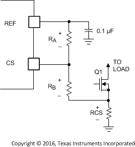 Figure 26. Biasing CS For Lower
Current-Sense Voltage
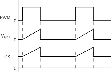 Figure 27. CS Pin Voltage with Biasing
The example shown uses a 200-mV full-scale signal at the current sense resistor. Resistor RB biases this up by approximately 700 mV to match the 0.9-V minimum specification of the current-limit comparator of the IC. The value of resistor RA changes with the specific IC used, due to the different reference voltages. The resistor values should be selected for minimal power loss. For example, a 50-µA bias current sets RB = 13 kΩ, and RA = 75 kΩ for UCCx813-[0,1,2,4] or RA = 56 kΩ for UCCx813-[3,5] devices.
8.3.12 Overcurrent Protection and Full-Cycle Restart
A separate overcurrent comparator within the UCCx813-x devices handles operation into a short-circuited or severely overloaded power supply output. This overcurrent comparator has a 1.5-V threshold and is also gated by the leading edge blanking signal to prevent false triggering. Once triggered, the overcurrent comparator uses the internal soft-start capacitor to generate a delay before retry is attempted. Often referred to as hiccup, this delay time is used to significantly reduce the input and dissipated power of the main converter and switching components. Full-cycle soft start ensures that there is a predictable delay of greater than 3 ms between successive attempts to operate during fault conditions. The circuit shown in Figure 28 and the timing diagram in Figure 29 show how the IC responds to a severe fault, such as a saturated inductor. When the peak current fault is first detected, the internal soft-start capacitor instantly discharges and stays discharged until the fault clears. At the same time, the PWM output is turned off and held off. When the fault clears, the capacitor slowly charges and allows the error amp output (COMP) to rise. When COMP gets high enough to enable the output, another fault occurs, latching off the PWM output, but the soft-start capacitor still continues to rise to 4 V before being discharged and permitting start of a new cycle. This means that for a severe fault, successive retries is spaced by the time required to fully charge the soft-start capacitor. TI recommends low leakage transformer designs in high-frequency applications to activate the overcurrent protection feature. Otherwise, the switch current may not ramp up sufficiently to trigger the overcurrent comparator within the leading edge blanking duration. This condition would cause continual cyclical triggering of the cycle-by-cycle current limit comparator but not the overcurrent comparator. This would result in brief high power dissipation durations in the main converter at the switching frequency. The intent of the overcurrent comparator is to reduce the effective retry rate under these conditions to a few milliseconds, thus significantly lowering the short-circuit power dissipation of the converter.
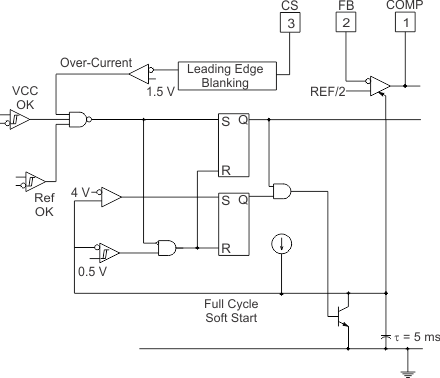 Figure 28. Detailed Block Diagram for Overcurrent Protection
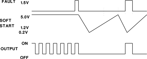 Figure 29. Device Behavior with Repetitive Fault at CS
8.3.13 Soft Start
Internal soft starting of the PWM output is accomplished by gradually increasing the error amplifier (E/A) output voltage at COMP. When used in current-mode control, this implementation slowly raises the peak switch current each PWM cycle in succession, forcing a controlled start-up. In voltage-mode (duty-cycle) control, this feature continually widens the pulse width.
Soft-start is performed within the UCCx813-x devices by clamping the E/A amplifier output (COMP) to the voltage on an internal soft-start capacitor (CSS), which is charged by a current source. CSS is discharged following an undervoltage lockout transition or if the reference voltage is below a minimum value for normal operation. Additionally, discharge of CSS occurs whenever the overcurrent protection comparator is triggered by a fault. The soft-start clamp circuitry is overridden once CSS charges above the voltage commanded by the error amplifier for normal PWM operation.
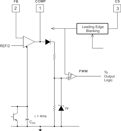 Figure 30. Detailed Block Diagram for Soft-Start
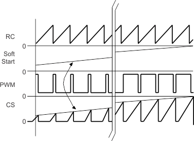 Figure 31. Device Soft-Start Behavior
8.3.14 Slope Compensation
Slope compensation can be added in all current-mode control applications to cancel the peak-to-average current error. Slope compensation is necessary in applications with duty-cycles exceeding 50%, but also improves performance in those below 50%. Primary current is sensed using resistor RCS in series with the converter switch. The timing resistor can be broken up into two series resistors to bias up an NPN voltage-follower, as shown in Figure 32. This is required to provide ample compliance for slope compensation at the beginning of a switching cycle, especially with continuous-current converters. The voltage follower drives the slope compensating programming resistor (RSC) to provide a slope-compensating current into CF.
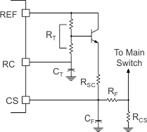 Figure 32. Adding Slope Compensation
8.4 Device Functional Modes
The UCCx813-x family of high-speed, low-power current-mode PWM controllers has the following functional modes.
8.4.1 Normal Operation
During this operation mode, the IC controls the power converter into the voltage-mode or current-mode control, regulates the output voltage or current through the converter duty cycle. The regulation can be achieve through the integrated error amplifier or external feedback circuitry.
8.4.2 UVLO Mode
During the system start-up, VVCC voltage starts to rise from 0 V. Before the VCC voltage reaches its corresponding turn-on threshold, the IC operates in UVLO mode. In this mode, REF pin voltage is not generated. When VVCC is above 1 V and below the turnon threshold, the REF pin is actively pulled low through a 5-kΩ resistor. This way, VREF can be used as a logic signal to indicate UVLO mode.
8.4.3 Soft-Start Mode
Once VCC voltage rises above the UVLO level, or the device comes out of a fault mode, it enters the soft-start mode. During soft-start, the internal soft-start capacitor CSS clamps the error amplifier output voltage, forcing it to rise slowly. This in turn controls the power converter peak current to rise slowly, reducing the voltage and current stress to the system. The UCCx813-x family has a fixed built-in soft-start time at 4 ms.
8.4.4 Fault Mode
A separate overcurrent comparator within the UCCx813-x devices handles operation into a short-circuited or severely overloaded power supply output. This overcurrent comparator has a 1.5-V threshold and is also gated by the leading-edge-blanking signal to prevent false triggering. When the fault is first detected, the internal soft-start capacitor instantly discharges and stays discharged until the fault clears. At the same time, the PWM output is turned off and held off. This is often referred to as hiccup. This delay time is used to significantly reduce the input and dissipated power of the main converter and switching components. Full-cycle soft-start insures that there is a predictable delay of greater than 3 milliseconds between successive attempts to operate during fault. When the fault clears, the capacitor slowly charges and allows the error amp output (COMP) to rise. When COMP gets high enough to enable the output, another fault occurs, latching off the PWM output, but the soft-start capacitor still continues to rise to 4 V before being discharged and permitting start of a new cycle. This means that for a severe fault, successive retries are spaced by the time required to fully charge the soft-start capacitor.