JAJS127E April 1999 – August 2016 UCC2813-0 , UCC2813-1 , UCC2813-2 , UCC2813-3 , UCC2813-4 , UCC2813-5 , UCC3813-0 , UCC3813-1 , UCC3813-2 , UCC3813-3 , UCC3813-4 , UCC3813-5
PRODUCTION DATA.
- 1 特長
- 2 アプリケーション
- 3 概要
- 4 改訂履歴
- 5 Device Comparison Table
- 6 Pin Configuration and Functions
- 7 Specifications
-
8 Detailed Description
- 8.1 Overview
- 8.2 Functional Block Diagram
- 8.3
Feature Description
- 8.3.1 Detailed Pin Descriptions
- 8.3.2 Undervoltage Lockout (UVLO)
- 8.3.3 Self-Biasing, Active Low Output
- 8.3.4 Reference Voltage
- 8.3.5 Oscillator
- 8.3.6 Synchronization
- 8.3.7 PWM Generator
- 8.3.8 Minimum Off-Time Adjustment (Dead-Time Control)
- 8.3.9 Leading Edge Blanking
- 8.3.10 Minimum Pulse Width
- 8.3.11 Current Limiting
- 8.3.12 Overcurrent Protection and Full-Cycle Restart
- 8.3.13 Soft Start
- 8.3.14 Slope Compensation
- 8.4 Device Functional Modes
-
9 Application and Implementation
- 9.1 Application Information
- 9.2
Typical Application
- 9.2.1 Design Requirements
- 9.2.2
Detailed Design Procedure
- 9.2.2.1 Bulk Capacitor Calculation
- 9.2.2.2 Transformer Design
- 9.2.2.3 MOSFET and Output Diode Selection
- 9.2.2.4 Output Capacitor Calculation
- 9.2.2.5 Current Sensing Network
- 9.2.2.6 Gate Drive Resistor
- 9.2.2.7 REF Bypass Capacitor
- 9.2.2.8 RT and CT
- 9.2.2.9 Start-Up Circuit
- 9.2.2.10 Voltage Feedback Compensation Procedure
- 9.2.3 Application Curves
- 10Power Supply Recommendations
- 11Layout
- 12デバイスおよびドキュメントのサポート
- 13メカニカル、パッケージ、および注文情報
パッケージ・オプション
デバイスごとのパッケージ図は、PDF版データシートをご参照ください。
メカニカル・データ(パッケージ|ピン)
- D|8
- PW|8
サーマルパッド・メカニカル・データ
発注情報
11 Layout
11.1 Layout Guidelines
In addition to following general power management IC layout guidelines (star grounding, minimal current loops, reasonable impedance levels, and so on) layout for the UCCx813-x family must consider the following:
- If possible, a ground plane should be used to minimize the voltage drop on the ground circuit and the noise introduced by parasitic inductances in individual traces.
- A decoupling capacitor is required for each the VCC pin and REF pin and both must be returned to GND as close to the IC as possible.
- For the best performance, keep the timing capacitor lead to GND as short and direct as possible. If possible, use separate ground traces for the timing capacitor and all other functions.
- The CS pin filter capacitor must be as close to the IC possible and grounded right at the IC ground pin. This ensures the best filtering effect and minimizes the chance of current sense pin malfunction.
- Gate-drive loop area must be minimized to reduce the EMI noise generated by the high di/dt of the current in the loop.
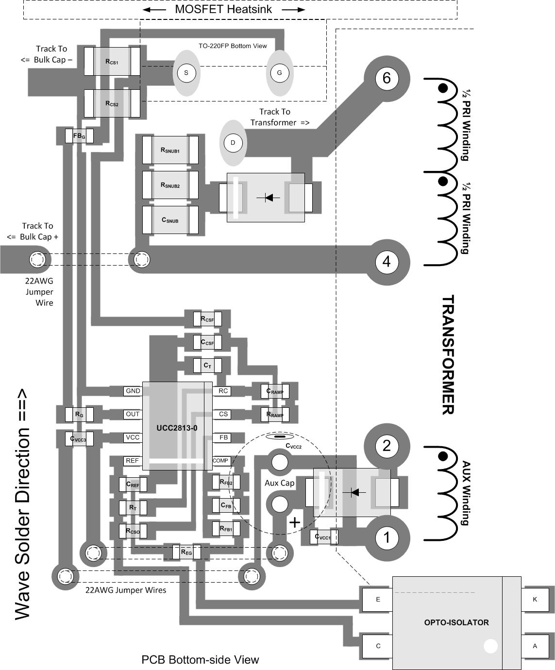
11.2 Layout Example
 Figure 44. UCC2813-0 Layout Example for Single-Layer PCB