JAJSKM1C october   2019  – september 2021 UCC5870-Q1

PRODUCTION DATA  

  1.   1
  2. 特長
  3. アプリケーション
  4. 概要
  5. Revision History
  6. Pin Configuration and Functions
  7. Specifications
    1. 6.1  Absolute Maximum Ratings
    2. 6.2  ESD Ratings
    3. 6.3  Recommended Operating Conditions
    4. 6.4  Thermal Information
    5. 6.5  Power Ratings
    6. 6.6  Insulation Specifications
    7. 6.7  Electrical Characteristics
    8. 6.8  SPI Timing Requirements
    9. 6.9  Switching Characteristics
    10. 6.10 Typical Characteristics
  8. Detailed Description
    1. 7.1 Overview
    2. 7.2 Functional Block Diagram
    3. 7.3 Feature Description
      1. 7.3.1 Power Supplies
        1. 7.3.1.1 VCC1
        2. 7.3.1.2 VCC2
        3. 7.3.1.3 VEE2
        4. 7.3.1.4 VREG1
        5. 7.3.1.5 VREG2
        6. 7.3.1.6 VREF
        7. 7.3.1.7 Other Internal Rails
      2. 7.3.2 Driver Stage
      3. 7.3.3 Integrated ADC for Front-End Analog (FEA) Signal Processing
        1. 7.3.3.1 AI* Setup
        2. 7.3.3.2 ADC Setup and Sampling Modes
          1. 7.3.3.2.1 Center Sampling Mode
          2. 7.3.3.2.2 Edge Sampling Mode
          3. 7.3.3.2.3 Hybrid Mode
        3. 7.3.3.3 DOUT Functionality
      4. 7.3.4 Fault and Warning Classification
      5. 7.3.5 Diagnostic Features
        1. 7.3.5.1  Undervoltage Lockout (UVLO) and Overvoltage Lockout (OVLO)
          1. 7.3.5.1.1 Built-In Self Test (BIST)
            1. 7.3.5.1.1.1 Analog Built-In Self Test (ABIST)
            2. 7.3.5.1.1.2 Function BIST
            3. 7.3.5.1.1.3 Clock Monitor
              1. 7.3.5.1.1.3.1 Clock Monitor Built-In Self Test
        2. 7.3.5.2  CLAMP, OUTH, and OUTL Clamping Circuits
        3. 7.3.5.3  Active Miller Clamp
        4. 7.3.5.4  DESAT based Short Circuit Protection (DESAT)
        5. 7.3.5.5  Shunt Resistor based Overcurrent Protection (OCP) and Short Circuit Protection (SCP)
        6. 7.3.5.6  Temperature Monitoring and Protection for the Power Transistors
        7. 7.3.5.7  Active High Voltage Clamping (VCECLP)
        8. 7.3.5.8  Two-Level Turn-Off
        9. 7.3.5.9  Soft Turn-Off (STO)
        10. 7.3.5.10 Thermal Shutdown (TSD) and Temperature Warning (TWN) of Driver IC
        11. 7.3.5.11 Active Short Circuit Support (ASC)
        12. 7.3.5.12 Shoot-Through Protection (STP)
        13. 7.3.5.13 Gate Voltage Monitoring and Status Feedback
        14. 7.3.5.14 VGTH Monitor
        15. 7.3.5.15 Cyclic Redundancy Check (CRC)
          1. 7.3.5.15.1 Calculating CRC
        16. 7.3.5.16 Configuration Data CRC
        17. 7.3.5.17 SPI Transfer Write/Read CRC
          1. 7.3.5.17.1 SDI CRC Check
          2. 7.3.5.17.2 SDO CRC Check
        18. 7.3.5.18 TRIM CRC Check
    4. 7.4 Device Functional Modes
      1. 7.4.1 State 1: RESET
      2. 7.4.2 State 2: Configuration 1
      3. 7.4.3 State 3: Configuration 2
      4. 7.4.4 State 4: Active
    5. 7.5 Programming
      1. 7.5.1 SPI Communication
        1. 7.5.1.1 System Configuration of SPI Communication
          1. 7.5.1.1.1 Independent Slave Configuration
          2. 7.5.1.1.2 Daisy Chain Configuration
          3. 7.5.1.1.3 Address-based Configuration
        2. 7.5.1.2 SPI Data Frame
          1. 7.5.1.2.1 Writing a Register
          2. 7.5.1.2.2 Reading a Register
    6. 7.6 Register Maps
      1. 7.6.1 UCC5870 Registers
  9. Applications and Implementation
    1. 8.1 Application Information
      1. 8.1.1 Power Dissipation Considerations
      2. 8.1.2 Device Addressing
    2. 8.2 Typical Application Using Internal ADC Reference and Power FET Sense Current Monitoring
      1. 8.2.1 Design Requirements
      2. 8.2.2 Detailed Design Procedure
        1. 8.2.2.1 VCC1, VCC2, and VEE2 Bypass Capacitors
        2. 8.2.2.2 VREF, VREG1, and VREG2 Bypass Capacitors
        3. 8.2.2.3 Bootstrap Capacitor (VBST)
        4. 8.2.2.4 VCECLP Input
        5. 8.2.2.5 External CLAMP Output
        6. 8.2.2.6 AI* Inputs
        7. 8.2.2.7 OUTH/ OUTL Outputs
        8. 8.2.2.8 nFLT* Outputs
      3. 8.2.3 Application Curves
    3. 8.3 Typical Application Using DESAT Power FET Monitoring
      1. 8.3.1 Detailed Design Procedure
        1. 8.3.1.1 DESAT Input
      2. 8.3.2 Application Curves
  10. Power Supply Recommendations
    1. 9.1 VCC1 Power Supply
    2. 9.2 VCC2 Power Supply
    3. 9.3 VEE2 Power Supply
    4. 9.4 VREF Supply (Optional)
  11. 10Layout
    1. 10.1 Layout Guidelines
      1. 10.1.1 Component Placement
      2. 10.1.2 Grounding Considerations
      3. 10.1.3 High-Voltage Considerations
      4. 10.1.4 Thermal Considerations
    2. 10.2 Layout Example
  12. 11Device and Documentation Support
    1. 11.1 Documentation Support
      1. 11.1.1 Related Documentation
    2. 11.2 Receiving Notification of Documentation Updates
    3. 11.3 サポート・リソース
    4. 11.4 Trademarks
    5. 11.5 静電気放電に関する注意事項
    6. 11.6 用語集
  13. 12Mechanical, Packaging, and Orderable Information

パッケージ・オプション

メカニカル・データ(パッケージ|ピン)
サーマルパッド・メカニカル・データ
発注情報

VCECLP Input

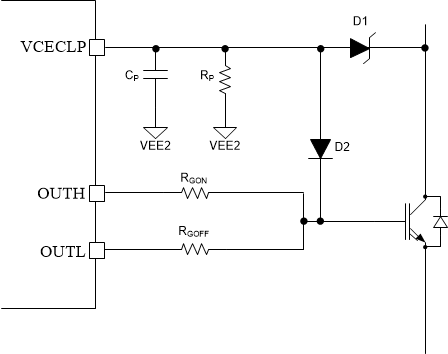
The active VCE clamp circuit is used to reduce VCE overshoot voltage during IGBT turn off. The external circuit (Figure 8-3) uses four components: A high-voltage TVS diode (D1) that turns on (avalanche breakdown) if the VCE overshoot during the IGBT turn-off is greater than the TVS diode avalanche limit, a filter capacitor (CP) that is charged when D1 conducts, a diode (D2) that conducts some of the avalanche current to the IGBT gate to increase the gate voltage (VGE) in order slow down the turn off transient and reduce the VCE overshoot, and a resistor (RC) to set the time constant to discharge the VCECLP node when D1 stops conducting. Select the D1 avalanche voltage rating to be the IGBT VCE overshoot voltage control target. During normal operation, the VCE dV/dt couples to VCECLP through junction capacitance of D1. The CP value is selected to filter this coupled ripple voltage to prevent triggering the VCE clamp function during normal operation. When a VCE over voltage occurs and D1 avalanches, CP charges to the VCECLPth by avalanche current, then VCE clamp function triggers and OUTL driver is disabled while the STO current is enabled. The RP value sets the the RC time constant when the CP voltage drops below VCECLPth. The value of RP depends on the selection of the IGBT, D1, RGON, RGOFF. Typically, the Rp value is between 10 to 100 ohm and CP value is between 10nF to 100nF. There is not a hard and fast calculation for these components. The best method is experimenting to fine tune the components for best performance in the application. See Figure 8-4 for an example of performance with the UCC5870QDWJEVM-026 (https://www.ti.com/tool/UCC5870QDWJEVM-026) EVM.
GUID-B920A302-FF6B-4A3E-8D4C-1A287C154062-low.pngFigure 8-3 VCECLP External Components