JAJS116J December 2003 – June 2022 TPS40054 , TPS40055 , TPS40057
PRODUCTION DATA
- 1 特長
- 2 アプリケーション
- 3 概要
- 4 Revision History
- 5 Pin Configuration and Functions
- 6 Specifications
-
7 Detailed Description
- 7.1 Overview
- 7.2 Functional Block Diagram
- 7.3
Feature Description
- 7.3.1 Setting the Switching Frequency (Programming the Clock Oscillator)
- 7.3.2 Programming The Ramp Generator Circuit
- 7.3.3 UVLO Operation
- 7.3.4 BP5 and BP10 Internal Voltage Regulators
- 7.3.5 Programming Soft Start
- 7.3.6 Programming Current Limit
- 7.3.7 Synchronizing to an External Supply
- 7.3.8 Loop Compensation
- 7.4 Device Functional Modes
-
8 Application and Implementation
- 8.1 Application Information
- 8.2
Typical Application
- 8.2.1 Design Requirements
- 8.2.2
Detailed Design Procedure
- 8.2.2.1 Calculate Maximum and Minimum Duty Cycles
- 8.2.2.2 Select Switching Frequency
- 8.2.2.3 Select ΔI
- 8.2.2.4 Calculate the High-Side MOSFET Power Losses
- 8.2.2.5 Calculate Synchronous Rectifier Losses
- 8.2.2.6 Calculate the Inductor Value
- 8.2.2.7 Set the Switching Frequency
- 8.2.2.8 Program the Ramp Generator Circuit
- 8.2.2.9 Calculate the Output Capacitance (CO)
- 8.2.2.10 Calculate the Soft-Start Capacitor (CSS/SD)
- 8.2.2.11 Calculate the Current Limit Resistor (RILIM)
- 8.2.2.12 Calculate Loop Compensation Values
- 8.2.2.13 Calculate the Boost and BP10V Bypass Capacitance
- 8.2.3 Application Curves
- 9 Power Supply Recommendations
- 10Layout
- 11Device and Documentation Support
- 12Mechanical, Packaging, and Orderable Information
8.1.5 High-Side MOSFET Power Dissipation
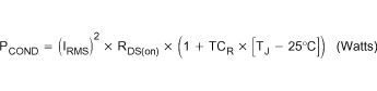
The power dissipated in the external high-side MOSFET is comprised of conduction and switching losses. The conduction losses are a function of the IRMS current through the MOSFET and the RDS(on) of the MOSFET. The high-side MOSFET conduction losses are defined by Equation 33.
where
- TCR is the temperature coefficient of the MOSFET RDS(on).
The TCR varies depending on MOSFET technology and manufacturer, but typically ranges between 3500 ppm/°C and 7000 ppm/°C.
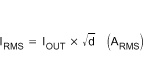
The IRMS current for the high-side MOSFET is described in Equation 34.
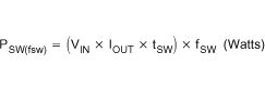
The switching losses for the high-side MOSFET are described in Equation 35.
where
- IO is the DC output current.
- tSW is the switching rise time, typically < 20 ns.
- fSW is the switching frequency.
Typical switching waveforms are shown in Figure 8-1.
 Figure 8-1 Inductor
Current and SW Node Waveforms
Figure 8-1 Inductor
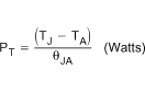
Current and SW Node WaveformsThe maximum allowable power dissipation in the MOSFET is determined by Equation 36.
where
- PT = PCOND + PSW(fsw) (W).
- θJA is the package thermal impedance.