JAJS116J December 2003 – June 2022 TPS40054 , TPS40055 , TPS40057
PRODUCTION DATA
- 1 特長
- 2 アプリケーション
- 3 概要
- 4 Revision History
- 5 Pin Configuration and Functions
- 6 Specifications
-
7 Detailed Description
- 7.1 Overview
- 7.2 Functional Block Diagram
- 7.3
Feature Description
- 7.3.1 Setting the Switching Frequency (Programming the Clock Oscillator)
- 7.3.2 Programming The Ramp Generator Circuit
- 7.3.3 UVLO Operation
- 7.3.4 BP5 and BP10 Internal Voltage Regulators
- 7.3.5 Programming Soft Start
- 7.3.6 Programming Current Limit
- 7.3.7 Synchronizing to an External Supply
- 7.3.8 Loop Compensation
- 7.4 Device Functional Modes
-
8 Application and Implementation
- 8.1 Application Information
- 8.2
Typical Application
- 8.2.1 Design Requirements
- 8.2.2
Detailed Design Procedure
- 8.2.2.1 Calculate Maximum and Minimum Duty Cycles
- 8.2.2.2 Select Switching Frequency
- 8.2.2.3 Select ΔI
- 8.2.2.4 Calculate the High-Side MOSFET Power Losses
- 8.2.2.5 Calculate Synchronous Rectifier Losses
- 8.2.2.6 Calculate the Inductor Value
- 8.2.2.7 Set the Switching Frequency
- 8.2.2.8 Program the Ramp Generator Circuit
- 8.2.2.9 Calculate the Output Capacitance (CO)
- 8.2.2.10 Calculate the Soft-Start Capacitor (CSS/SD)
- 8.2.2.11 Calculate the Current Limit Resistor (RILIM)
- 8.2.2.12 Calculate Loop Compensation Values
- 8.2.2.13 Calculate the Boost and BP10V Bypass Capacitance
- 8.2.3 Application Curves
- 9 Power Supply Recommendations
- 10Layout
- 11Device and Documentation Support
- 12Mechanical, Packaging, and Orderable Information
8.1.1 Selecting the Inductor Value
The inductor value determines the magnitude of ripple current in the output capacitors as well as the load current at which the converter enters discontinuous mode. Too large an inductance results in lower ripple current but is physically larger for the same load current. An inductance that is too small results in larger ripple currents and a greater number of (or more expensive output capacitors for) the same output ripple voltage requirement. A good compromise is to select the inductance value such that the converter does not enter discontinuous mode until the load approximated somewhere between 10% and 30% of the rated output. The inductance value is described in Equation 24.
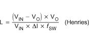
where
- VO is the output voltage.
- ΔI is the peak-to-peak inductor current.