JAJS116J December 2003 – June 2022 TPS40054 , TPS40055 , TPS40057
PRODUCTION DATA
- 1 特長
- 2 アプリケーション
- 3 概要
- 4 Revision History
- 5 Pin Configuration and Functions
- 6 Specifications
-
7 Detailed Description
- 7.1 Overview
- 7.2 Functional Block Diagram
- 7.3
Feature Description
- 7.3.1 Setting the Switching Frequency (Programming the Clock Oscillator)
- 7.3.2 Programming The Ramp Generator Circuit
- 7.3.3 UVLO Operation
- 7.3.4 BP5 and BP10 Internal Voltage Regulators
- 7.3.5 Programming Soft Start
- 7.3.6 Programming Current Limit
- 7.3.7 Synchronizing to an External Supply
- 7.3.8 Loop Compensation
- 7.4 Device Functional Modes
-
8 Application and Implementation
- 8.1 Application Information
- 8.2
Typical Application
- 8.2.1 Design Requirements
- 8.2.2
Detailed Design Procedure
- 8.2.2.1 Calculate Maximum and Minimum Duty Cycles
- 8.2.2.2 Select Switching Frequency
- 8.2.2.3 Select ΔI
- 8.2.2.4 Calculate the High-Side MOSFET Power Losses
- 8.2.2.5 Calculate Synchronous Rectifier Losses
- 8.2.2.6 Calculate the Inductor Value
- 8.2.2.7 Set the Switching Frequency
- 8.2.2.8 Program the Ramp Generator Circuit
- 8.2.2.9 Calculate the Output Capacitance (CO)
- 8.2.2.10 Calculate the Soft-Start Capacitor (CSS/SD)
- 8.2.2.11 Calculate the Current Limit Resistor (RILIM)
- 8.2.2.12 Calculate Loop Compensation Values
- 8.2.2.13 Calculate the Boost and BP10V Bypass Capacitance
- 8.2.3 Application Curves
- 9 Power Supply Recommendations
- 10Layout
- 11Device and Documentation Support
- 12Mechanical, Packaging, and Orderable Information
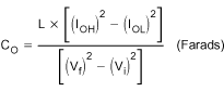
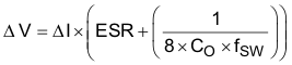
8.1.2 Calculating the Output Capacitance
The output capacitance depends on the output ripple voltage requirement, output ripple current, as well as any output voltage deviation requirement during a load transient.
The output ripple voltage is a function of both the output capacitance and capacitor ESR. The worst-case output ripple is described in Equation 25.
where
- CO is the output capacitance.
- ESR is the equivalent series resistance of the output capacitance.
The output ripple voltage is typically between 90% and 95% due to the ESR component.
The output capacitance requirement typically increases in the presence of a load transient requirement. During a step load, the output capacitance must provide energy to the load (light to heavy load step) or absorb excess inductor energy (heavy to light load step) while maintaining the output voltage within acceptable limits. The amount of capacitance depends on the magnitude of the load step, the speed of the loop, and the size of the inductor.
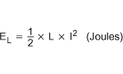
Stepping the load from a heavy load to a light load results in an output overshoot. Excess energy stored in the inductor must be absorbed by the output capacitance. The energy stored in the inductor is described in Equation 26.
where
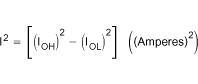
- IOH is the output current under heavy load conditions.
- IOL is the output current under light load conditions.
Energy in the capacitor is described in Equation 28.
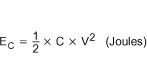
where
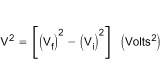
where
- Vf is the final peak capacitor voltage.
- Vi is the initial capacitor voltage.
Substituting Equation 27 into Equation 26, then substituting Equation 29 into Equation 28, then setting Equation 28 equal to Equation 26, and then solving for CO yields the capacitance described in Equation 30.