JAJS116J December 2003 – June 2022 TPS40054 , TPS40055 , TPS40057
PRODUCTION DATA
- 1 特長
- 2 アプリケーション
- 3 概要
- 4 Revision History
- 5 Pin Configuration and Functions
- 6 Specifications
-
7 Detailed Description
- 7.1 Overview
- 7.2 Functional Block Diagram
- 7.3
Feature Description
- 7.3.1 Setting the Switching Frequency (Programming the Clock Oscillator)
- 7.3.2 Programming The Ramp Generator Circuit
- 7.3.3 UVLO Operation
- 7.3.4 BP5 and BP10 Internal Voltage Regulators
- 7.3.5 Programming Soft Start
- 7.3.6 Programming Current Limit
- 7.3.7 Synchronizing to an External Supply
- 7.3.8 Loop Compensation
- 7.4 Device Functional Modes
-
8 Application and Implementation
- 8.1 Application Information
- 8.2
Typical Application
- 8.2.1 Design Requirements
- 8.2.2
Detailed Design Procedure
- 8.2.2.1 Calculate Maximum and Minimum Duty Cycles
- 8.2.2.2 Select Switching Frequency
- 8.2.2.3 Select ΔI
- 8.2.2.4 Calculate the High-Side MOSFET Power Losses
- 8.2.2.5 Calculate Synchronous Rectifier Losses
- 8.2.2.6 Calculate the Inductor Value
- 8.2.2.7 Set the Switching Frequency
- 8.2.2.8 Program the Ramp Generator Circuit
- 8.2.2.9 Calculate the Output Capacitance (CO)
- 8.2.2.10 Calculate the Soft-Start Capacitor (CSS/SD)
- 8.2.2.11 Calculate the Current Limit Resistor (RILIM)
- 8.2.2.12 Calculate Loop Compensation Values
- 8.2.2.13 Calculate the Boost and BP10V Bypass Capacitance
- 8.2.3 Application Curves
- 9 Power Supply Recommendations
- 10Layout
- 11Device and Documentation Support
- 12Mechanical, Packaging, and Orderable Information
8.1.6 Synchronous Rectifier MOSFET Power Dissipation
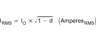
The power dissipated in the synchronous rectifier MOSFET is comprised of three components: RDS(on) conduction losses, body diode conduction losses, and reverse recovery losses. RDS(on) conduction losses can be defined using Equation 31 and the RMS current through the synchronous rectifier MOSFET is described in Equation 37.
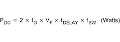
The body-diode conduction losses are due to forward conduction of the body diode during the anti-cross conduction delay time. The body diode conduction losses are described by Equation 38.
where
- VF is the body diode forward voltage.
- tDELAY is the delay time just before the SW node rises.
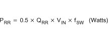
The 2-multiplier is used because the body diode conducts twice during each cycle (once on the rising edge and once on the falling edge). The reverse recovery losses are due to the time it takes for the body diode to recover from a forward bias to a reverse blocking state. The reverse recovery losses are described in Equation 39.
where
- QRR is the reverse recovery charge of the body diode.
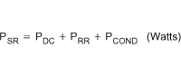
The QRR is not always described in a MOSFET data sheet, but can be obtained from the MOSFET vendor. The total synchronous rectifier MOSFET power dissipation is described in Equation 40.