JAJSBF8B June 2011 – April 2018 TPS54478
PRODUCTION DATA.
- 1 特長
- 2 アプリケーション
- 3 概要
- 4 改訂履歴
- 5 Pin Configuration and Functions
- 6 Specifications
-
7 Detailed Description
- 7.1 Overview
- 7.2 Functional Block Diagram
- 7.3
Feature Description
- 7.3.1 Fixed Frequency PWM Control
- 7.3.2 Slope Compensation and Output Current
- 7.3.3 Bootstrap Voltage (BOOT) and Low Dropout Operation
- 7.3.4 Error Amplifier
- 7.3.5 Voltage Reference
- 7.3.6 Adjusting the Output Voltage
- 7.3.7 Enable and Adjusting Undervoltage Lockout
- 7.3.8 Slow Start / Tracking Pin
- 7.3.9 Constant Switching Frequency and Timing Resistor (RT/CLK Pin)
- 7.3.10 Overcurrent Protection
- 7.3.11 START-UP into Prebiased Output
- 7.3.12 Synchronize Using the RT/CLK Pin
- 7.3.13 Power Good (PWRGD Pin)
- 7.3.14 Overvoltage Transient Protection
- 7.3.15 Thermal Shutdown
- 7.3.16 Small Signal Model for Loop Response
- 7.3.17 Simple Small Signal Model for Peak Current Mode Control
- 7.3.18 Small Signal Model for Frequency Compensation
- 7.4 Device Functional Modes
- 7.5 Programming
- 8 Application and Implementation
- 9 Power Supply Recommendations
- 10Layout
- 11デバイスおよびドキュメントのサポート
- 12メカニカル、パッケージ、および注文情報
6.6 Typical Characteristics
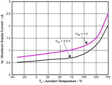 Figure 1. Shutdown Supply Current vs Temperature
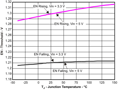 Figure 3. EN Pin Voltage vs Temperature
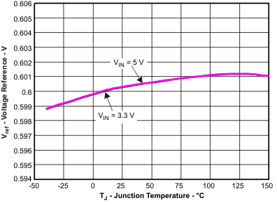 Figure 5. Voltage Reference vs Temperature
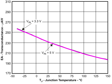 Figure 7. Transconductance vs Temperature
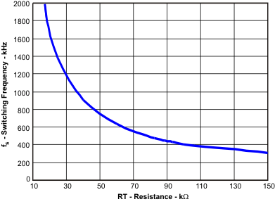 Figure 9. Switching Frequency vs RT Resistance
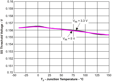 Figure 11. VSS Voltage Threshold VSSTHR vs Temperature
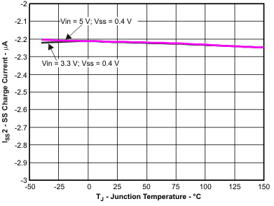 Figure 13. SS Charge Current vs Temperature
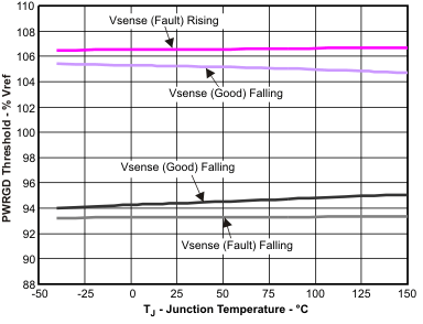 Figure 15. PWRGD Threshold vs Temperature
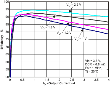 Figure 17. Efficiency vs Load Current
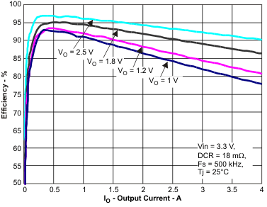 Figure 19. Efficiency vs Load Current
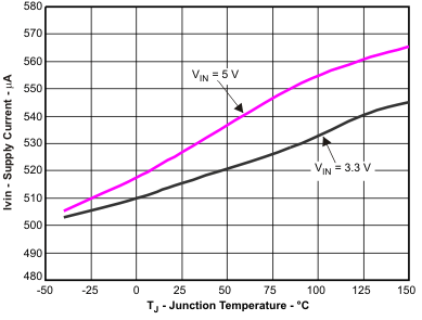 Figure 2. VIN Supply Current vs Temperature
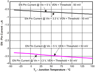 Figure 4. EN Pin Current vs Temperature
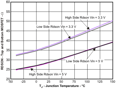 Figure 6. MOSFET Rdson vs Temperature
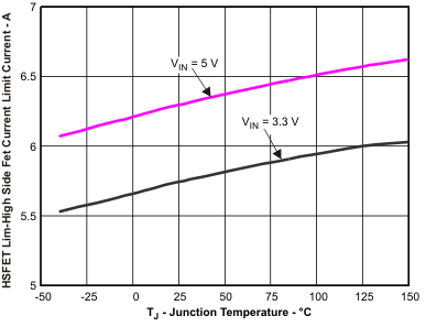 Figure 8. High Side FET Current Limit vs Temperature
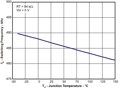 Figure 10. Switching Frequency vs Temperature
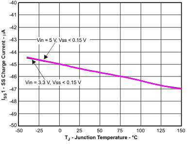 Figure 12. SS Charge Current vs Temperature
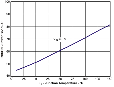 Figure 14. PWRGD Rdson vs Temperature
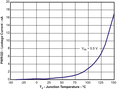 Figure 16. PWRGD Leakage Current vs Temperature
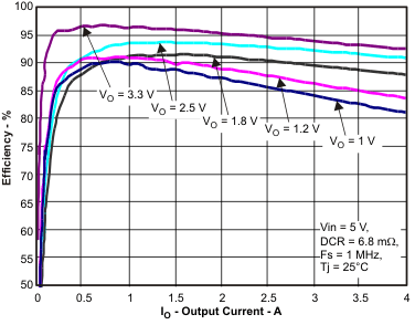 Figure 18. Efficiency vs Load Current
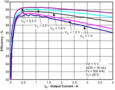 Figure 20. Efficiency vs Load Current