JAJSBF8B June 2011 – April 2018 TPS54478
PRODUCTION DATA.
- 1 特長
- 2 アプリケーション
- 3 概要
- 4 改訂履歴
- 5 Pin Configuration and Functions
- 6 Specifications
-
7 Detailed Description
- 7.1 Overview
- 7.2 Functional Block Diagram
- 7.3
Feature Description
- 7.3.1 Fixed Frequency PWM Control
- 7.3.2 Slope Compensation and Output Current
- 7.3.3 Bootstrap Voltage (BOOT) and Low Dropout Operation
- 7.3.4 Error Amplifier
- 7.3.5 Voltage Reference
- 7.3.6 Adjusting the Output Voltage
- 7.3.7 Enable and Adjusting Undervoltage Lockout
- 7.3.8 Slow Start / Tracking Pin
- 7.3.9 Constant Switching Frequency and Timing Resistor (RT/CLK Pin)
- 7.3.10 Overcurrent Protection
- 7.3.11 START-UP into Prebiased Output
- 7.3.12 Synchronize Using the RT/CLK Pin
- 7.3.13 Power Good (PWRGD Pin)
- 7.3.14 Overvoltage Transient Protection
- 7.3.15 Thermal Shutdown
- 7.3.16 Small Signal Model for Loop Response
- 7.3.17 Simple Small Signal Model for Peak Current Mode Control
- 7.3.18 Small Signal Model for Frequency Compensation
- 7.4 Device Functional Modes
- 7.5 Programming
- 8 Application and Implementation
- 9 Power Supply Recommendations
- 10Layout
- 11デバイスおよびドキュメントのサポート
- 12メカニカル、パッケージ、および注文情報
7.3.12 Synchronize Using the RT/CLK Pin
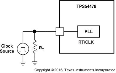
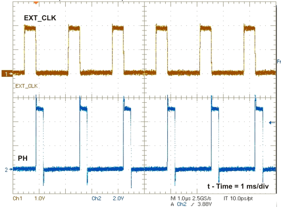
The RT/CLK pin is used to synchronize the converter to an external system clock. See Figure 29. To implement the synchronization feature in a system, connect a square wave to the RT/CLK pin with an on time of at least 75ns. If the pin is pulled above the PLL upper threshold, a mode change occurs and the pin becomes a synchronization input. The internal amplifier is disabled and the pin is a high impedance clock input to the internal PLL. If clocking edges stop, the internal amplifier is re-enabled and the mode returns to the frequency set by the resistor. The square wave amplitude at this pin must transition lower than 0.6 V and higher than 1.6 V typically. The synchronization frequency range is 300 kHz to 2000 kHz. The rising edge of the PH is synchronized to the falling edge of RT/CLK pin.
 Figure 29. Synchronizing to a System Clock
 Figure 30. Plot of Synchronizing to System Clock