JAJSBF8B June 2011 – April 2018 TPS54478
PRODUCTION DATA.
- 1 特長
- 2 アプリケーション
- 3 概要
- 4 改訂履歴
- 5 Pin Configuration and Functions
- 6 Specifications
-
7 Detailed Description
- 7.1 Overview
- 7.2 Functional Block Diagram
- 7.3
Feature Description
- 7.3.1 Fixed Frequency PWM Control
- 7.3.2 Slope Compensation and Output Current
- 7.3.3 Bootstrap Voltage (BOOT) and Low Dropout Operation
- 7.3.4 Error Amplifier
- 7.3.5 Voltage Reference
- 7.3.6 Adjusting the Output Voltage
- 7.3.7 Enable and Adjusting Undervoltage Lockout
- 7.3.8 Slow Start / Tracking Pin
- 7.3.9 Constant Switching Frequency and Timing Resistor (RT/CLK Pin)
- 7.3.10 Overcurrent Protection
- 7.3.11 START-UP into Prebiased Output
- 7.3.12 Synchronize Using the RT/CLK Pin
- 7.3.13 Power Good (PWRGD Pin)
- 7.3.14 Overvoltage Transient Protection
- 7.3.15 Thermal Shutdown
- 7.3.16 Small Signal Model for Loop Response
- 7.3.17 Simple Small Signal Model for Peak Current Mode Control
- 7.3.18 Small Signal Model for Frequency Compensation
- 7.4 Device Functional Modes
- 7.5 Programming
- 8 Application and Implementation
- 9 Power Supply Recommendations
- 10Layout
- 11デバイスおよびドキュメントのサポート
- 12メカニカル、パッケージ、および注文情報
8.2.3 Application Curves
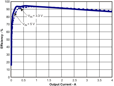 Figure 38. Efficiency vs Load Current
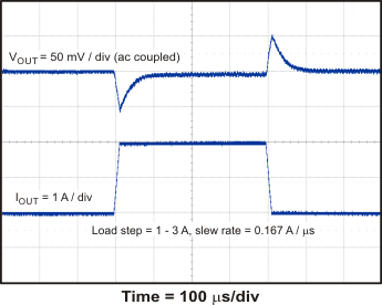 Figure 40. Transient Response, 2 A Step
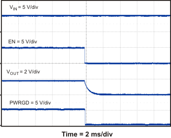 Figure 42. Power Up VOUT, EN
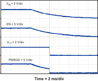 Figure 44. Power Down VOUT, VIN
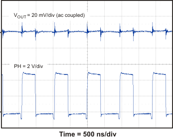 Figure 46. Output Ripple, IOUT = 4 A
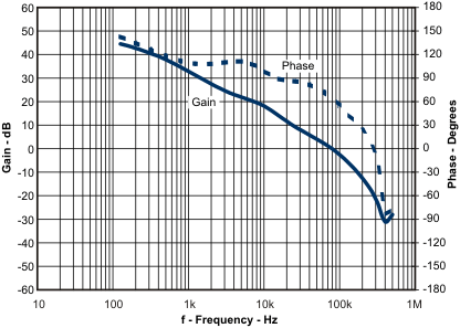 Figure 48. Closed Loop Response, VIN = 5 V, IOUT = 4 A
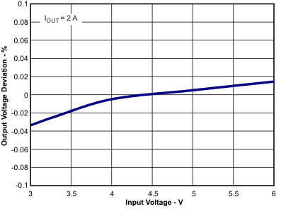 Figure 50. Output Voltage Regulation vs Input Voltage
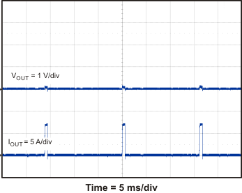 Figure 52. Hiccup Mode Current Limit
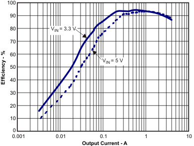 Figure 39. Efficiency vs Load Current
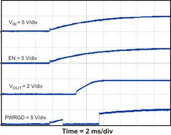 Figure 41. Power Up VOUT, VIN
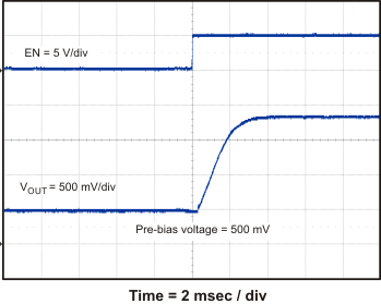 Figure 43. Power Up into Prebias Voltage
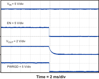 Figure 45. Power Down VOUT, EN
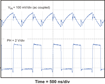 Figure 47. Input Ripple, IOUT = 4 A
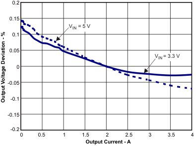 Figure 49. Output Voltage Regulation vs Load Current
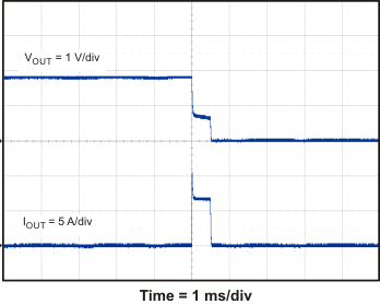 Figure 51. Hiccup Mode Current Limit
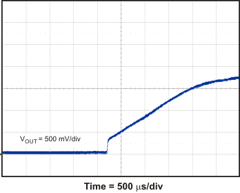 Figure 53. Start Up Characteristic