JAJSI70C May 2008 – November 2019 DAC9881
PRODUCTION DATA.
- 1 特長
- 2 アプリケーション
- 3 概要
- 4 改訂履歴
- 5 概要(続き)
- 6 Pin Configuration and Functions
-
7 Specifications
- 7.1 Absolute Maximum Ratings
- 7.2 ESD Ratings
- 7.3 Recommended Operating Conditions
- 7.4 Thermal Information
- 7.5 Electrical Characteristics: AVDD = 5 V
- 7.6 Electrical Characteristics: AVDD = 2.7 V
- 7.7 Timing Requirements—Standalone Operation Without SDO
- 7.8 Timing Requirements—Standalone Operation With SDO and Daisy-Chain Mode
- 7.9 Typical Characteristics: AVDD = 5 V
- 7.10 Typical Characteristics: AVDD = 2.7 V
-
8 Detailed Description
- 8.1 Overview
- 8.2 Functional Block Diagram
- 8.3 Feature Description
- 8.4 Device Functional Modes
- 9 Application and Implementation
- 10Power Supply Recommendations
- 11Layout
- 12デバイスおよびドキュメントのサポート
- 13メカニカル、パッケージ、および注文情報
7.8 Timing Requirements—Standalone Operation With SDO and Daisy-Chain Mode
at –40°C to +105°C (unless otherwise noted); see Figure 2 and Figure 3(1)(2)(3)| MIN | MAX | UNIT | |||
|---|---|---|---|---|---|
| fSCLK | Maximum clock frequency | 2.7 ≤ AVDD < 3.6 V, 2.7 ≤ IOVDD ≤ AVDD | 20 | MHz | |
| 3.6 ≤ AVDD ≤ 5.5 V, 2.7 ≤ IOVDD ≤ AVDD | 25 | MHz | |||
| t1 | Minumum CS high time | 2.7 ≤ AVDD < 3.6 V, 2.7 ≤ IOVDD ≤ AVDD | 50 | ns | |
| 3.6 ≤ AVDD ≤ 5.5 V, 2.7 ≤ IOVDD ≤ AVDD | 30 | ns | |||
| t2 | Delay from CS falling edge to SCLK rising edge | 2.7 ≤ AVDD < 3.6 V, 2.7 ≤ IOVDD ≤ AVDD | 10 | ns | |
| 3.6 ≤ AVDD ≤ 5.5 V, 2.7 ≤ IOVDD ≤ AVDD | 8 | ns | |||
| t3 | Delay from SCLK falling edge to CS falling edge | 2.7 ≤ AVDD < 3.6 V, 2.7 ≤ IOVDD ≤ AVDD | 0 | ns | |
| 3.6 ≤ AVDD ≤ 5.5 V, 2.7 ≤ IOVDD ≤ AVDD | 0 | ns | |||
| t4 | SCLK low time | 2.7 ≤ AVDD < 3.6 V, 2.7 ≤ IOVDD ≤ AVDD | 25 | ns | |
| 3.6 ≤ AVDD ≤ 5.5 V, 2.7 ≤ IOVDD ≤ AVDD | 20 | ns | |||
| t5 | SCLK high time | 2.7 ≤ AVDD < 3.6 V, 2.7 ≤ IOVDD ≤ AVDD | 25 | ns | |
| 3.6 ≤ AVDD ≤ 5.5 V, 2.7 ≤ IOVDD ≤ AVDD | 20 | ns | |||
| t6 | SCLK cycle time | 2.7 ≤ AVDD < 3.6 V, 2.7 ≤ IOVDD ≤ AVDD | 50 | ns | |
| 3.6 ≤ AVDD ≤ 5.5 V, 2.7 ≤ IOVDD ≤ AVDD | 40 | ns | |||
| t7 | Delay from SCLK rising edge to CS rising edge | 2.7 ≤ AVDD < 3.6 V, 2.7 ≤ IOVDD ≤ AVDD | 10 | ns | |
| 3.6 ≤ AVDD ≤ 5.5 V, 2.7 ≤ IOVDD ≤ AVDD | 10 | ns | |||
| t8 | Input data setup time | 2.7 ≤ AVDD < 3.6 V, 2.7 ≤ IOVDD ≤ AVDD | 5 | ns | |
| 3.6 ≤ AVDD ≤ 5.5 V, 2.7 ≤ IOVDD ≤ AVDD | 5 | ns | |||
| t9 | Input data hold time | 2.7 ≤ AVDD < 3.6 V, 2.7 ≤ IOVDD ≤ AVDD | 5 | ns | |
| 3.6 ≤ AVDD ≤ 5.5 V, 2.7 ≤ IOVDD ≤ AVDD | 5 | ns | |||
| t10 | Delay from CS falling edge to SDO valid | 2.7 ≤ AVDD < 3.6 V, 2.7 ≤ IOVDD ≤ AVDD | 15 | ns | |
| 3.6 ≤ AVDD ≤ 5.5 V, 2.7 ≤ IOVDD ≤ AVDD | 10 | ns | |||
| t11 | Delay from SCLK falling edge to SDO valid | 2.7 ≤ AVDD < 3.6 V, 2.7 ≤ IOVDD ≤ AVDD | 20 | ns | |
| 3.6 ≤ AVDD ≤ 5.5 V, 2.7 ≤ IOVDD ≤ AVDD | 15 | ns | |||
| t12 | SDO data hold from SCLK rising edge | 2.7 ≤ AVDD < 3.6 V, 2.7 ≤ IOVDD ≤ AVDD | t5 | ns | |
| 3.6 ≤ AVDD ≤ 5.5 V, 2.7 ≤ IOVDD ≤ AVDD | t5 | ns | |||
| t13 | Delay from CS rising edge to SDO high-Z | 2.7 ≤ AVDD < 3.6 V, 2.7 ≤ IOVDD ≤ AVDD | 8 | ns | |
| 3.6 ≤ AVDD ≤ 5.5 V, 2.7 ≤ IOVDD ≤ AVDD | 5 | ns | |||
| t14 | Delay from CS rising edge to LDAC falling edge | 2.7 ≤ AVDD < 3.6 V, 2.7 ≤ IOVDD ≤ AVDD | 10 | ns | |
| 3.6 ≤ AVDD ≤ 5.5 V, 2.7 ≤ IOVDD ≤ AVDD | 5 | ns | |||
| t15 | LDAC pulse width | 2.7 ≤ AVDD < 3.6 V, 2.7 ≤ IOVDD ≤ AVDD | 15 | ns | |
| 3.6 ≤ AVDD ≤ 5.5 V, 2.7 ≤ IOVDD ≤ AVDD | 10 | ns | |||
(1) All input signals are specified with tR = tF = 2ns (10% to 90% of IOVDD) and timed from a voltage level of IOVDD / 2.
(2) Specified by design; not production tested.
(3) Sample tested during the initial release and after any redesign or process changes that may affect these parameters.
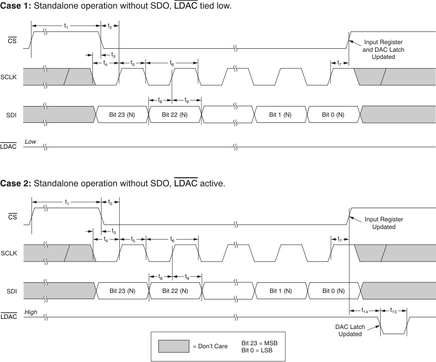
 Figure 1. Timing Diagram for Standalone Operation Without SDO
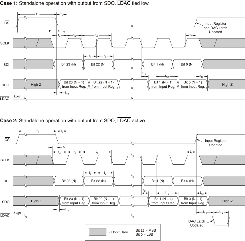
  Figure 2. Timing Diagram for Standalone Operation With SDO
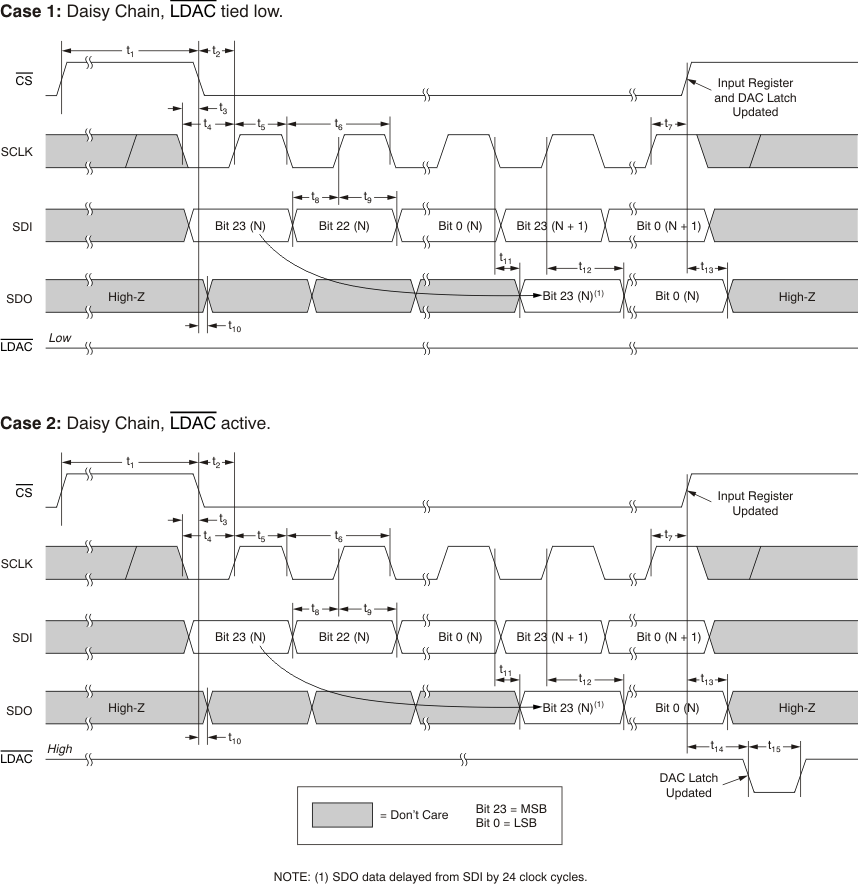
  Figure 3. Timing Diagram for Daisy-Chain Mode, Two Cascaded Devices