JAJU878 November   2022 ADS117L11 , ADS127L11


  1.   概要
  2.   リソース
  3.   特長
  4.   アプリケーション
  5.   5
  6. 1System Description
    1. 1.1 Key System Specification
  7. 2System Overview
    1. 2.1 Block Diagram
    2. 2.2 Design Considerations
      1. 2.2.1 Signal-Chain Voltage Levels
        1.       12
      2. 2.2.2 ADC Configuration
      3. 2.2.3 ADC Clocking and Synchronization
      4. 2.2.4 Differential Low-Pass Filter
      5. 2.2.5 Current Source
      6. 2.2.6 Gain Stage and High-Pass Filter
    3. 2.3 Highlighted Products
      1. 2.3.1 ADS127L11
      2. 2.3.2 THS4551
  8. 3System Design Theory
    1. 3.1 IEPE Sensor
      1. 3.1.1 IEPE Sensor Parameters
        1. 3.1.1.1 Sensitivity and Measurement Range
        2. 3.1.1.2 Excitation, Output Bias Voltage, and Output Impedance
        3. 3.1.1.3 Linearity and Temperature Variance
        4. 3.1.1.4 Frequency Response
        5. 3.1.1.5 Noise and Dynamic Range
  9. 4Hardware, Software, Testing, and Test Results
    1. 4.1 Hardware Description
      1. 4.1.1 Board Interface
      2. 4.1.2 Power Configuration
        1. 4.1.2.1 Power Sequence
        2. 4.1.2.2 Analog Supply
        3. 4.1.2.3 Digital Supply
        4. 4.1.2.4 Excitation Current Supply
        5. 4.1.2.5 SPI Connectivity Modes and Their Assembly Variants
          1. 4.1.2.5.1 Daisy-Chain Mode
          2. 4.1.2.5.2 Parallel SDO Mode
          3. 4.1.2.5.3 Parallel SDI Mode and Parallel SDO Mode
          4. 4.1.2.5.4 Clocking Modes
    2. 4.2 Software Requirements
    3. 4.3 Test Setup and Procedure
      1. 4.3.1 Noise Floor and SNR
      2. 4.3.2 Gain and Input Range
      3. 4.3.3 Crosstalk
      4. 4.3.4 Total Harmonic Distortion
      5. 4.3.5 Clock Image Rejection
      6. 4.3.6 Synchronization of the ADCs
      7. 4.3.7 Fault Detection Circuit
    4. 4.4 Test Results
      1. 4.4.1 Noise Floor and Dynamic Range
      2. 4.4.2 Gain and Input Range
      3. 4.4.3 Crosstalk
      4. 4.4.4 Total Harmonic Distortion
      5. 4.4.5 Clock Image Rejection
      6. 4.4.6 Synchronization of the ADCs
      7. 4.4.7 Fault Detection Circuit
      8. 4.4.8 Test With Actual IEPE Sensor
      9. 4.4.9 Measurement Results Summary
  10. 5Design and Documentation Support
    1. 5.1 Design Files
      1. 5.1.1 Schematics
      2. 5.1.2 BOM
    2. 5.2 Software
    3. 5.3 Documentation Support
    4. 5.4 サポート・リソース
    5. 5.5 Trademarks
  11. 6About the Author
Clocking Modes

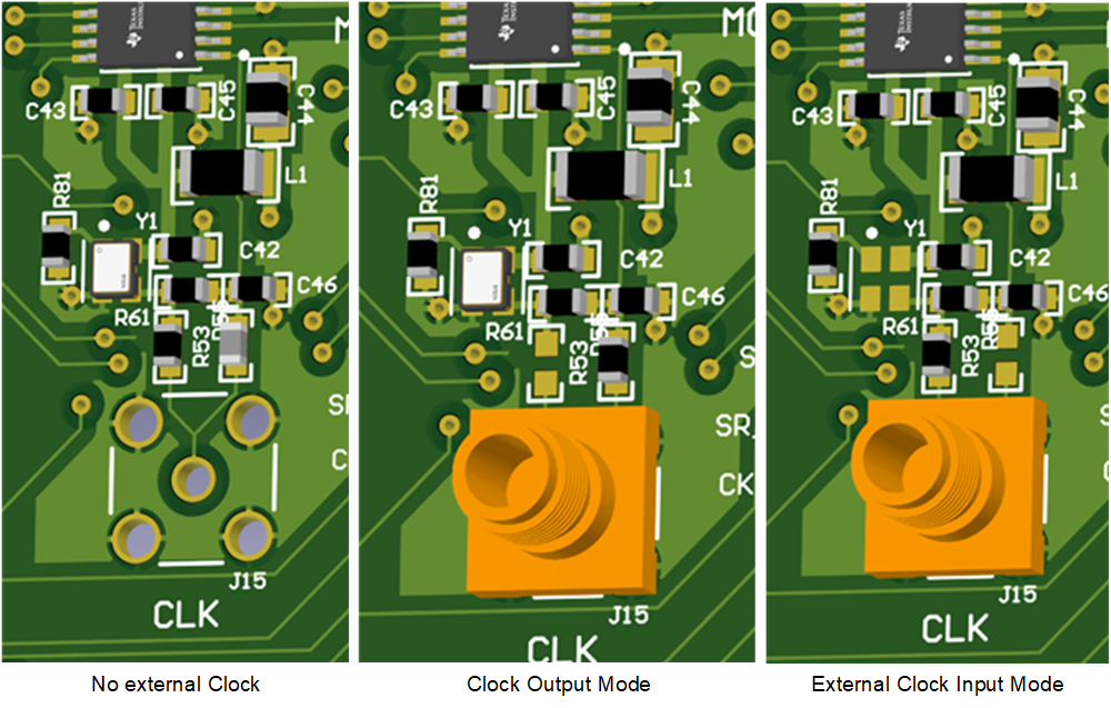
The board supports 3 clocking modes as illustrated in Figure 4-6:

  1. Stand-alone mode: there is no clock line connection to other boards
  2. Clock output mode: the onboard clock is connected to the SMA connector
  3. External clock input mode: there is no onboard clock, the external clock is connected to the SMA connector

Table 4-2 details the board configuration with a minor assembly variant in the clocking section.

Table 4-2 Board Clocking Configurations
NO EXTERNAL CLOCK CONNECTIVITY CLOCK OUTPUT MODE EXTERNAL CLOCK INPUT MODE
J15 removed R53 removed Y1 removed, R55 removed
GUID-20220829-SS0I-CGDF-FCKT-F426FHT118DP-low.png Figure 4-6 Clocking Assembly Variants

If synchronizing two boards, configure the first board in clock output mode, and configure the second board in external clock input mode. A short coaxial cable connects J15 on both boards, and both boards can be connected to the same controller. Use the controller to handle the difference in nRDY signal.