JAJU878 November   2022 ADS117L11 , ADS127L11


  1.   概要
  2.   リソース
  3.   特長
  4.   アプリケーション
  5.   5
  6. 1System Description
    1. 1.1 Key System Specification
  7. 2System Overview
    1. 2.1 Block Diagram
    2. 2.2 Design Considerations
      1. 2.2.1 Signal-Chain Voltage Levels
        1.       12
      2. 2.2.2 ADC Configuration
      3. 2.2.3 ADC Clocking and Synchronization
      4. 2.2.4 Differential Low-Pass Filter
      5. 2.2.5 Current Source
      6. 2.2.6 Gain Stage and High-Pass Filter
    3. 2.3 Highlighted Products
      1. 2.3.1 ADS127L11
      2. 2.3.2 THS4551
  8. 3System Design Theory
    1. 3.1 IEPE Sensor
      1. 3.1.1 IEPE Sensor Parameters
        1. 3.1.1.1 Sensitivity and Measurement Range
        2. 3.1.1.2 Excitation, Output Bias Voltage, and Output Impedance
        3. 3.1.1.3 Linearity and Temperature Variance
        4. 3.1.1.4 Frequency Response
        5. 3.1.1.5 Noise and Dynamic Range
  9. 4Hardware, Software, Testing, and Test Results
    1. 4.1 Hardware Description
      1. 4.1.1 Board Interface
      2. 4.1.2 Power Configuration
        1. 4.1.2.1 Power Sequence
        2. 4.1.2.2 Analog Supply
        3. 4.1.2.3 Digital Supply
        4. 4.1.2.4 Excitation Current Supply
        5. 4.1.2.5 SPI Connectivity Modes and Their Assembly Variants
          1. 4.1.2.5.1 Daisy-Chain Mode
          2. 4.1.2.5.2 Parallel SDO Mode
          3. 4.1.2.5.3 Parallel SDI Mode and Parallel SDO Mode
          4. 4.1.2.5.4 Clocking Modes
    2. 4.2 Software Requirements
    3. 4.3 Test Setup and Procedure
      1. 4.3.1 Noise Floor and SNR
      2. 4.3.2 Gain and Input Range
      3. 4.3.3 Crosstalk
      4. 4.3.4 Total Harmonic Distortion
      5. 4.3.5 Clock Image Rejection
      6. 4.3.6 Synchronization of the ADCs
      7. 4.3.7 Fault Detection Circuit
    4. 4.4 Test Results
      1. 4.4.1 Noise Floor and Dynamic Range
      2. 4.4.2 Gain and Input Range
      3. 4.4.3 Crosstalk
      4. 4.4.4 Total Harmonic Distortion
      5. 4.4.5 Clock Image Rejection
      6. 4.4.6 Synchronization of the ADCs
      7. 4.4.7 Fault Detection Circuit
      8. 4.4.8 Test With Actual IEPE Sensor
      9. 4.4.9 Measurement Results Summary
  10. 5Design and Documentation Support
    1. 5.1 Design Files
      1. 5.1.1 Schematics
      2. 5.1.2 BOM
    2. 5.2 Software
    3. 5.3 Documentation Support
    4. 5.4 サポート・リソース
    5. 5.5 Trademarks
  11. 6About the Author
Daisy-Chain Mode

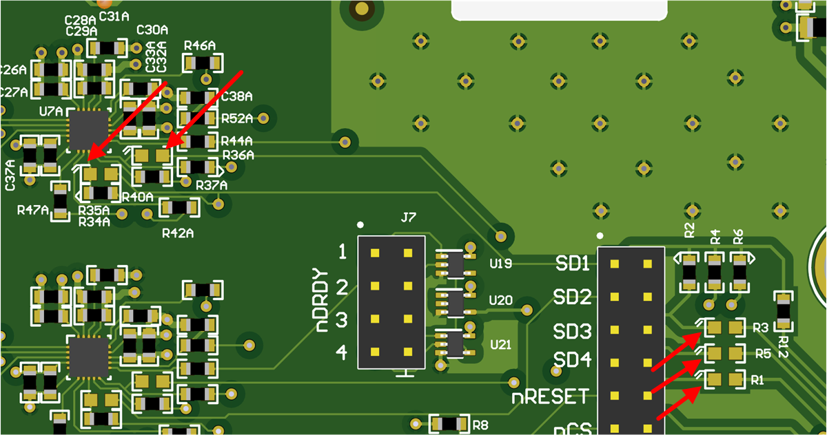
In this mode, the four ADCs are connected in a daisy-chain fashion Figure 4-3 shows. The maximum SPI clock rate in this mode is 16 MHz.

The following board assembly is required to enable the daisy-chain mode:

  • R40x, R36x (all channels), remove R3, R5, and R1
Note: Figure 4-3 shows that all of those resistors are indicated by small parallel lines on the top left corner of the resistor.
GUID-20220829-SS0I-RQQC-3WDB-CX3VP9Q3VHCQ-low.pngFigure 4-3 Daisy-Chain Variant