JAJU878 November   2022 ADS117L11 , ADS127L11


  1.   概要
  2.   リソース
  3.   特長
  4.   アプリケーション
  5.   5
  6. 1System Description
    1. 1.1 Key System Specification
  7. 2System Overview
    1. 2.1 Block Diagram
    2. 2.2 Design Considerations
      1. 2.2.1 Signal-Chain Voltage Levels
        1.       12
      2. 2.2.2 ADC Configuration
      3. 2.2.3 ADC Clocking and Synchronization
      4. 2.2.4 Differential Low-Pass Filter
      5. 2.2.5 Current Source
      6. 2.2.6 Gain Stage and High-Pass Filter
    3. 2.3 Highlighted Products
      1. 2.3.1 ADS127L11
      2. 2.3.2 THS4551
  8. 3System Design Theory
    1. 3.1 IEPE Sensor
      1. 3.1.1 IEPE Sensor Parameters
        1. 3.1.1.1 Sensitivity and Measurement Range
        2. 3.1.1.2 Excitation, Output Bias Voltage, and Output Impedance
        3. 3.1.1.3 Linearity and Temperature Variance
        4. 3.1.1.4 Frequency Response
        5. 3.1.1.5 Noise and Dynamic Range
  9. 4Hardware, Software, Testing, and Test Results
    1. 4.1 Hardware Description
      1. 4.1.1 Board Interface
      2. 4.1.2 Power Configuration
        1. 4.1.2.1 Power Sequence
        2. 4.1.2.2 Analog Supply
        3. 4.1.2.3 Digital Supply
        4. 4.1.2.4 Excitation Current Supply
        5. 4.1.2.5 SPI Connectivity Modes and Their Assembly Variants
          1. 4.1.2.5.1 Daisy-Chain Mode
          2. 4.1.2.5.2 Parallel SDO Mode
          3. 4.1.2.5.3 Parallel SDI Mode and Parallel SDO Mode
          4. 4.1.2.5.4 Clocking Modes
    2. 4.2 Software Requirements
    3. 4.3 Test Setup and Procedure
      1. 4.3.1 Noise Floor and SNR
      2. 4.3.2 Gain and Input Range
      3. 4.3.3 Crosstalk
      4. 4.3.4 Total Harmonic Distortion
      5. 4.3.5 Clock Image Rejection
      6. 4.3.6 Synchronization of the ADCs
      7. 4.3.7 Fault Detection Circuit
    4. 4.4 Test Results
      1. 4.4.1 Noise Floor and Dynamic Range
      2. 4.4.2 Gain and Input Range
      3. 4.4.3 Crosstalk
      4. 4.4.4 Total Harmonic Distortion
      5. 4.4.5 Clock Image Rejection
      6. 4.4.6 Synchronization of the ADCs
      7. 4.4.7 Fault Detection Circuit
      8. 4.4.8 Test With Actual IEPE Sensor
      9. 4.4.9 Measurement Results Summary
  10. 5Design and Documentation Support
    1. 5.1 Design Files
      1. 5.1.1 Schematics
      2. 5.1.2 BOM
    2. 5.2 Software
    3. 5.3 Documentation Support
    4. 5.4 サポート・リソース
    5. 5.5 Trademarks
  11. 6About the Author

Fault Detection Circuit

Sweeping the input voltage results in the following thresholds for a fault-detection circuit:

  • 0.5 V is the short detection threshold
  • 20.1 V is the open detection threshold

The input signal stepped down from 10 V to 0 V, and the output of the short detection comparator is probed. The plot in Figure 4-19 shows a delay of 1.5 ms until the comparator output goes low.
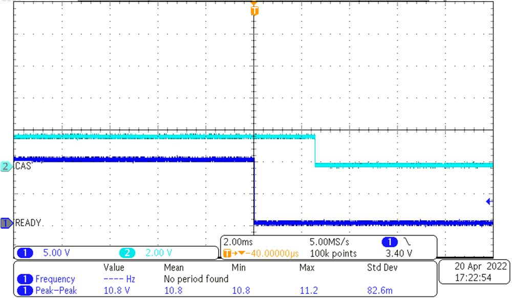
GUID-20220829-SS0I-09B2-CXCB-80HCDN8MHQJK-low.png Figure 4-19 Time-Domain Plot of Fault Detection Circuit Delay