SBAA461 December 2020 ADC3541 , ADC3542 , ADC3543 , ADC3544 , ADC3641 , ADC3642 , ADC3643 , ADC3644 , ADC3660 , ADC3681 , ADC3682 , ADC3683
2.2.3 0.5 Wire
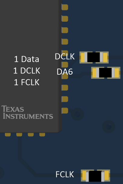
In 1/2 Wire mode (only applicable to 2CH ADCs), all 14 bits of two channels are being transmitted on one wire. With the DCLK and FCLK, there is a total of 3 output pins/resistors.
 Figure 2-9 ADC3643 Serial CMOS: 0.5 Wire
Resistors
Figure 2-9 ADC3643 Serial CMOS: 0.5 Wire
ResistorsA total of 28 bits (14 bits from CHA and 14 bits from CHB) are being transmitted on one wire over one frame clock period, so the serialization rate is 28x. The data rate is limited to ~250 due to the CMOS interface, so the max sampling rate in this mode is 8.9 MSPS. Higher sampling rates can be used when decimation is utilized.
| Mode | Max Sampling Rate (MSPS) | Serialization Rate | Data Rate (Mbps) | Data Outputs/ Resistors |
|---|---|---|---|---|
| 1 Wire | 8.9 | 28 | 250 | 4 |
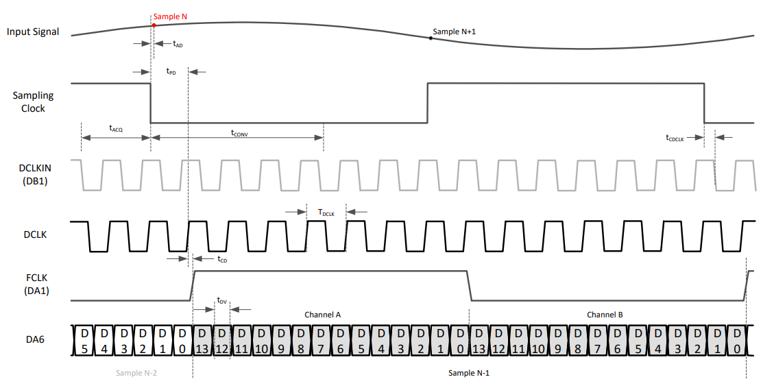
 Figure 2-10 Serial CMOS 0.5W Timing
Diagram
Figure 2-10 Serial CMOS 0.5W Timing
DiagramIn summary of CMOS serial interfaces, we can see that there is a tradeoff to be made between the number of data outputs/resistors, and the maximum data rate.
| Max Sampling Rate (MSPS) | Serialization Rate | Data Rate (Mbps) | Data Pins/ Resistors | |
|---|---|---|---|---|
| 2 Wire | 35.7 | 7 | 250 | 6 |
| 1 Wire | 17.8 | 14 | 250 | 4 |
| 1/2 Wire | 8.9 | 28 | 250 | 3 |