SBAU269C October   2016  – August 2021 ADS8900B


  1.   Trademarks
  2. 1EVM Overview
    1. 1.1 ADS8900EVM-PDK Kit Features
    2. 1.2 ADS8900EVM Features
  3. 2Analog Interface
    1. 2.1 ADS8900B Connections and Decoupling
    2. 2.2 ADC Amplifier Input Drive
    3. 2.3 Voltage Reference and VCM Scaling
  4. 3Digital Interface
    1. 3.1 multiSPI™ for ADC Digital I/O
    2. 3.2 I2C Bus for Onboard EEPROM
  5. 4Power Supplies
    1. 4.1 Positive Supply and Test Points
    2. 4.2 Negative Supply
  6. 5ADS8900EVM-PDK Initial Setup
    1. 5.1 Software Installation
    2. 5.2 Default Jumper Settings for Differential Inputs
    3. 5.3 Default Jumpers for Bipolar, Single-Ended Inputs
    4. 5.4 Default Jumpers for Unipolar, Single-Ended Inputs
    5. 5.5 External Source Requirements for ADS8900 Evaluation
  7. 6ADS8900EVM-PDK Operation
    1. 6.1 EVM GUI Global Settings for ADC Control
    2. 6.2 Register Map Configuration Tool
    3. 6.3 Time Domain Display Tool
    4. 6.4 Spectral Analysis Tool
    5. 6.5 Histogram Tool
    6. 6.6 Linearity Analysis Tool
    7. 6.7 ADS8900BEVM Support for ADS8910B and ADS8920B Devices
  8. 7Bill of Materials, PCB Layout, and Schematics
    1. 7.1 Bill of Materials (BOM)
    2. 7.2 PCB Layout
    3. 7.3 Schematics
  9. 8Revision History

Negative Supply

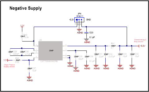
The negative supply, as shown in Figure 4-2, is not installed on the EVM but can be populated in the rare circumstance that this option is desired. The purpose of this negative charge pump is to generate a small –0.23-V power-supply rail for the FDA driver amplifier to assure that the amplifier can swing to 0 V without an output swing limitation. This feature is needed to run the linearity sweep for the EVM because the linearity test requires a linear sinusoidal input signal that drives below 0 V and above 5 V (that is, a saturated input). Without the negative charge pump, the THS4551 amplifier distorts when its output approaches 0 V.
GUID-20201202-CA0I-BDJ0-NJLK-C3PDD7HZT796-low.gifFigure 4-2 Negative Supply