SBAU269C October 2016 – August 2021 ADS8900B
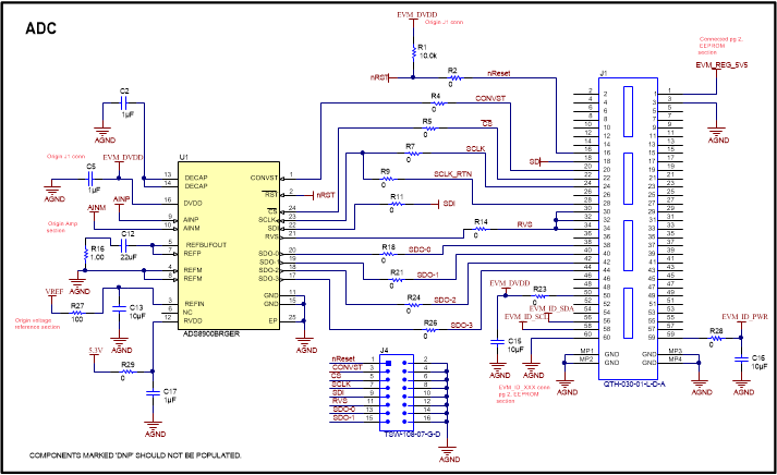
2.1 ADS8900B Connections and Decoupling
Figure 2-1 shows the power-supply connections, reference connections, and the associated
decoupling filter capacitors for the ADS8900. The reference filter comprised of C12 and
R16 is at the reference buffer output and must be as close as possible to the ADC
reference pin (pin 7). This figure also shows the analog input connections, but the
driver amplifier is in Figure 2-2. The digital signal connections are shown on the right hand side of Figure 2-1. The connector J4 is a test point header that can be used to monitor digital signals.
Also, J4 can be used to apply digital signals in cases where the included PHI controller
is not used. Each digital signal has a series 0-Ω resistor. This resistor can be changed
to a 50-Ω resistor to provide signal conditioning for noisy digital signals. The
included PHI controller digital signals do not require this conditioning so the default
value is 0 Ω. Figure 2-1 also shows the PHI connector, J1. This connector provides the SPI digital signals,
power supplies, and I2C communications for the EVM.
 Figure 2-1 Decoupling and ADC Signal
Connections
 Figure 2-1 Decoupling and ADC Signal
Connections