SBOA367B December 2019 – June 2022 TLV9001 , TLV9002 , TLV9004 , TLV9051 , TLV9052 , TLV9054 , TLV9061 , TLV9062 , TLV9064
- Designing for TLV90xxS operational amplifiers with shutdown
- Trademarks
- 1 Introduction
- 2 Shutdown Specifications
- 3 SHDN Pin Limits and Connections
- 4 Output Behavior During Enable and Shutdown
- 5 Enable Time and Shutdown Time Factors
- 6 Impact on Commonly Used Circuit Configurations
- 7 Advanced Circuit Functionality Using Amplifiers With Shutdown
- 8 Conclusion
- 9 References
- 10Revision History
5.3 Load
Another important factor in determining the shutdown time of an amplifier is the output load. When the amplifier is disabled via the SHDN pin, there is some amount of charge available at the output pin. This output charge corresponds to the output voltage and is dependent on the load seen at the output. When the amplifier is in the shutdown state, the load is effectively comprised of the loading components, the feedback components, and the parasitic components seen at the amplifier’s inputs and outputs. To complete the shutdown process, the output charge must dissipate so the output voltage may transition from the previous output voltage to the shutdown output voltage. Because this charge dissipates through the load, the shutdown time is dependent on the load component(s).
With this in mind, consider the following three scenarios for an amplifier in a unity gain buffer configuration: a purely resistive load, no load, and a purely capacitive load. Figure 5-1 displays an example graphic for this scenario. On the left is the amplifier during normal operation. On the right is the effective circuit which models the amplifier’s behavior while the part is in shutdown. CCM and CID model the common mode input capacitance and the differential input capacitance of the amplifier. CSHDN and RSHDN represent the output impedance of the part while in shutdown.
 Figure 5-1 Buffer Circuit
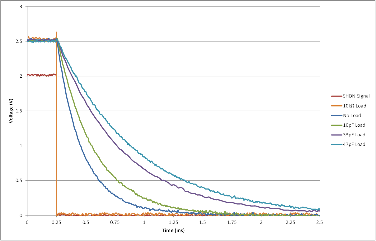
In the case where the load component, ZLOAD, is purely resistive and much smaller than RSHDN, 10 kΩ for example, the amplifier will experience the fastest shutdown time for the three types of output loads. This is because the output charge is established only by the relatively small parasitic capacitances of the part, such as CSHDN, and this charge has a purely resistive pulldown path to ground via the output load. The expected output signal during shutdown would look like a fast RC response from the starting output voltage to ground.
In the case where there is no output load, the output charge stored on the parasitic capacitances would still be relatively small. However, the charge would have to be displaced to ground through the very large RSHDN, which forms a significant RC combination with the parasitic capacitances, or through parasitic and leakage paths in the amplifier. Thus, the expected shutdown time would be significantly longer for this load scenario. Note that parasitic board capacitance can contribute to this parasitic output capacitance.
The worst-case of the three scenarios, however, would be a purely capacitive load. For this case, even a typical load of 10 pF could significantly increase the time taken by the part to fully shut down. Under this condition, the output charge would be significantly higher than before with both the parasitic and load capacitances now storing output charge. Additionally, the load capacitor would further increase the size of the RC combination formed by RSHDN and CSHDN and offer no lower resistive path to ground. Consequently, the amplifier would take a long time to displace the charge stored at the output.
Figure 5-2 shows the shutdown times for the aforementioned configurations. All data was gathered using a TLV9062S on a 5-V single-supply in a unity buffer gain configuration with a 2.5-V input. The SHDN pin of channel 1 was toggled while channel 2 was left on. Note that the 10-kΩ load shutdown time is much faster than the other load times and that the curve nearly overlaps with the SHDN pin signal curve on this time scale.
 Figure 5-2 Load and Shutdown TLV9062S
| Output Load | Enable Time | Shutdown Time |
|---|---|---|
| 10 kΩ | 5.20 µs | 604 ns |
| No Load | 5.20 µs | 536 µs |
| 10 pF | 5.20 µs | 752 µs |
| 33 pF | 5.20 µs | 1.35 ms |
| 47 pF | 5.20 µs | 1.61 ms |