SBOK049 November 2023 OPA4H014-SEP
PRODUCTION DATA
4.2 Input Offset Voltage Parametric Shift
Input offset voltage (VOS) for the OPA4H014-SEP is specified as ±30 μV typical and ±120 μV maximum at TA = 25°C. The input offset voltage was measured at multiple supply voltages, with test limits of ±100 μV for guardbanding purposes.
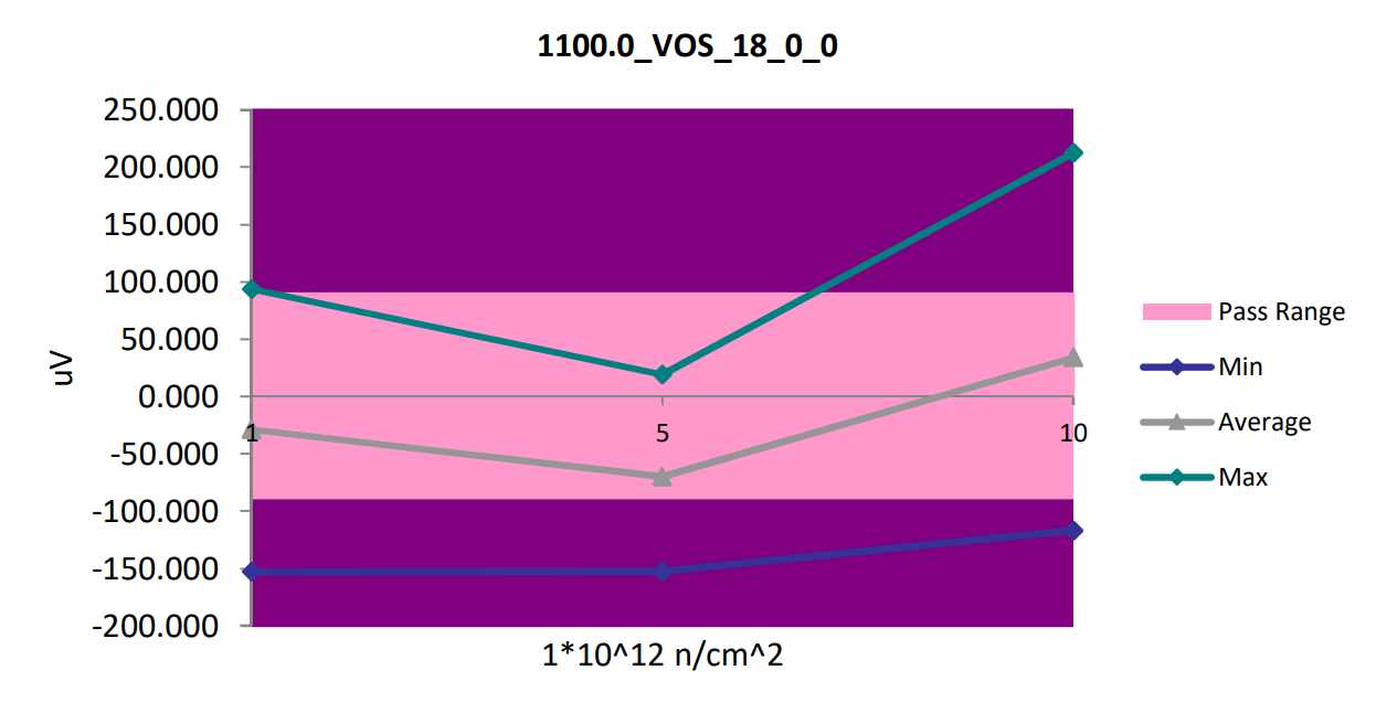
All but one of the devices exposed to neutron irradiation were found to have a measured input offset voltage outside of the specified data sheet limits, across all four device amplifier channels, for at least one of the VOS tests performed on the ATE. Values reported below are from one example test with VS = ±9 V (test numbers 1100.0-1103.0). Full data for all ATE tests performed are included in the report appendix.
- Of the three samples tested to 1 × 10¹² n/cm2, a mean post-irradiation VOS magnitude of 68 μV and maximum post-irradiation VOS magnitude of 152.94 μV were recorded. Only the sample with serial number 1 did not exhibit a parametric shift to a level in excess of the data sheet specification on any channel.
- Of the three samples tested to 5 × 10¹² n/cm2, a mean post-irradiation VOS magnitude of 110.67 μV and maximum post-irradiation VOS magnitude of 284.55 μV were recorded.
- Of the three samples tested to 1 × 10¹³ n/cm2, a mean post-irradiation VOS magnitude of 186.82 μV and maximum post-irradiation VOS magnitude of 508.11 μV were recorded.
 Figure 4-2 Sample Input Offset Voltage
NDD Graph