SBOU236A February 2020 – March 2021
7.2 PCB Layout
The ALM2403Q1EVM is a four-layer PCB design. Figure 7-2 to Figure 7-6 show the PCB layer illustrations. The top layer consists of all signal path traces, and is poured with a solid ground plane. A symmetrical board layout is used on amplifier 1 and amplifier 2 to keep good performance matching. Decoupling capacitors C4, C5, and C10 are positioned on the top layer as close as possible to the power supply pins of the device. The second internal layer is a dedicated solid GND plane. Independent vias are placed at the ground connection of every component to provide a low-impedance path to ground. The third internal layer and the bottom layer route the power-supply connections.
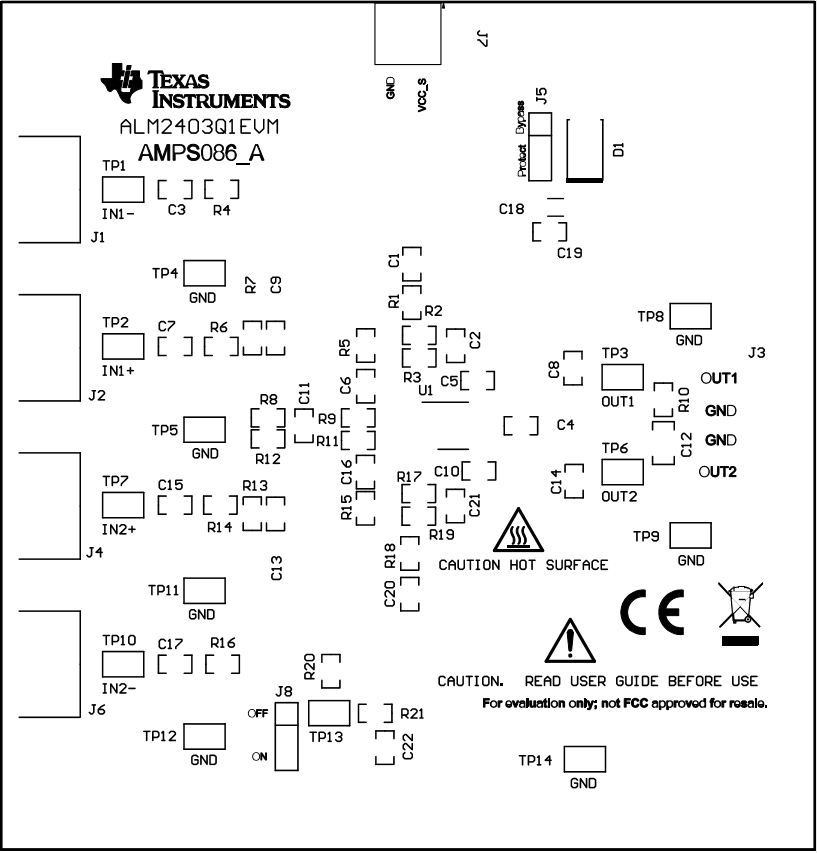 Figure 7-2 Top
Overlay PCB Layout
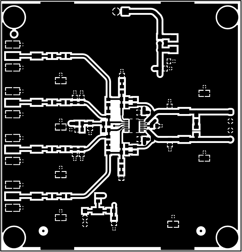 Figure 7-3 Top Layer
PCB Layout
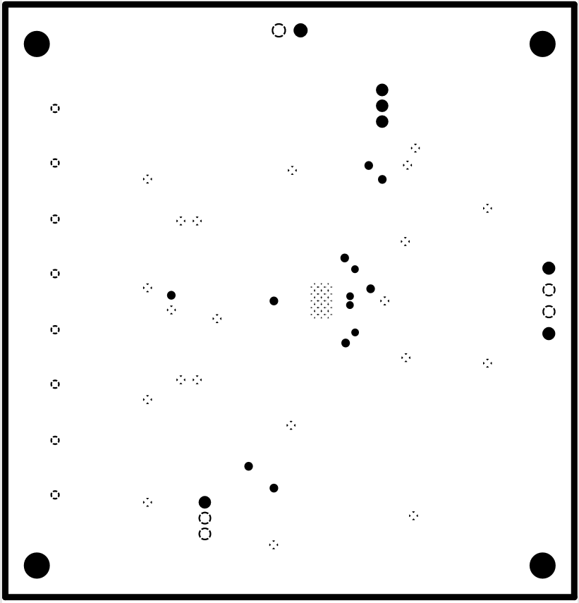 Figure 7-4 Ground
Layer PCB Layout
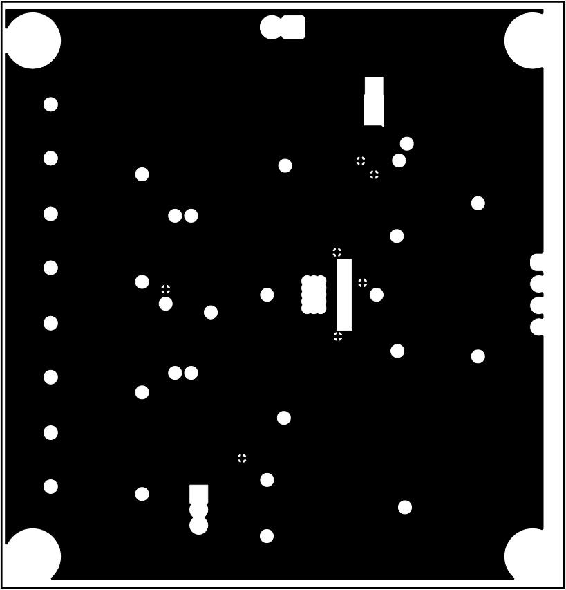 Figure 7-5 Power
Layer PCB Layout
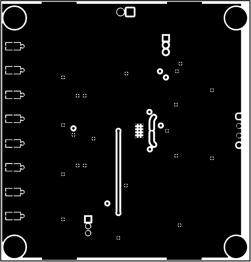 Figure 7-6 Bottom
Layer PCB Layout