SLAAEF9 November   2023 MSPM0L1306


  1.   1
  2.   Abstract
  3.   Trademarks
  4. 1MSPM0 Portfolio Overview
    1. 1.1 Introduction
    2. 1.2 Portfolio Comparison of Renesas RL78 MCUs to MSPM0 MCUs
  5. 2Ecosystem And Migration
    1. 2.1 Ecosystem Comparison
      1. 2.1.1 MSPM0 Software Development Kit (MSPM0 SDK)
      2. 2.1.2 The IDE Supported By MSPM0
      3. 2.1.3 SysConfig
      4. 2.1.4 Debug Tools
      5. 2.1.5 LaunchPad
    2. 2.2 Migration Process
      1. 2.2.1 Step 1. Choose The Right MSPM0 MCU
      2. 2.2.2 Step 2. Set Up IDE And Quick Introduction of CCS
        1. 2.2.2.1 Set Up IDE
        2. 2.2.2.2 Quick Introduction of CCS
      3. 2.2.3 Step 3. Set Up MSPM0 SDK And Quick Introduction of MSPM0 SDK
        1. 2.2.3.1 Set Up MSPM0 SDK
        2. 2.2.3.2 Quick Introduction of SDK
      4. 2.2.4 Step 4. Software Evaluation
      5. 2.2.5 Step 5. PCB Board Design
      6. 2.2.6 Step 6. Mass Production
    3. 2.3 Example
  6. 3Core Architecture Comparison
    1. 3.1 CPU
    2. 3.2 Embedded Memory Comparison
      1. 3.2.1 Flash Features
      2. 3.2.2 Flash Organization
        1. 3.2.2.1 Flash Memory Regions
        2. 3.2.2.2 NONMAIN Memory of MSPM0
        3. 3.2.2.3 Flash Memory Registers of RL78
      3. 3.2.3 Embedded SRAM
    3. 3.3 Power UP and Reset Summary and Comparison
    4. 3.4 Clocks Summary and Comparison
      1. 3.4.1 Oscillators
        1. 3.4.1.1 MSPM0 Oscillators
      2. 3.4.2 Clock Signal Comparison
    5. 3.5 MSPM0 Operating Modes Summary and Comparison
      1. 3.5.1 Operating Modes Comparison
      2. 3.5.2 MSPM0 Capabilities in Lower Modes
      3. 3.5.3 Entering Lower-Power Modes
      4. 3.5.4 Low-Power Mode Code Examples
    6. 3.6 Interrupts and Events Comparison
      1. 3.6.1 Interrupts and Exceptions
        1. 3.6.1.1 Interrupt Management of RL78
        2. 3.6.1.2 Interrupt Management of MSPM0
      2. 3.6.2 Event Handler of MSPM0
      3. 3.6.3 Event Link Controller (ELC) of RL78
      4. 3.6.4 Event Management Comparison
    7. 3.7 Debug and Programming Comparison
      1. 3.7.1 Debug Comparison
      2. 3.7.2 Programming Mode Comparison
        1. 3.7.2.1 Bootstrap Loader (BSL) Programming of MSPM0
        2. 3.7.2.2 Serial Programming (Using External Device) of RL78
  7. 4Digital Peripheral Comparison
    1. 4.1 General-Purpose I/O (GPIO, IOMUX)
    2. 4.2 Universal Asynchronous Receiver-Transmitter (UART)
    3. 4.3 Serial Peripheral Interface (SPI)
    4. 4.4 Inter-Integrated Circuit (I2C)
    5. 4.5 Timers (TIMGx, TIMAx)
    6. 4.6 Windowed Watchdog Timer (WWDT)
    7. 4.7 Real-Time Clock (RTC)
  8. 5Analog Peripheral Comparison
    1. 5.1 Analog-to-Digital Converter (ADC)
    2. 5.2 Comparator (COMP)
    3. 5.3 Digital-to-Analog Converter (DAC)
    4. 5.4 Operational Amplifier (OPA)
    5. 5.5 Voltage References (VREF)

Event Handler of MSPM0

MSPM0 MCUs have an event manager that transfers digital events from one entity to another. The event manager implements event transfer through a defined set of event publishers (generators) and subscribers (receivers) that are interconnected through an event fabric containing a combination of static and programmable routes. The event manger can also perform handshaking with the power management and clock unit (PMCU), to make sure that the necessary clock and power domain are present for triggered event actions to take place.

Events that are transferred by the event manager include:

  • Peripheral event transferred to the CPU as an interrupt request (IRQ)
  • Peripheral event transferred to the DMA as a DMA trigger
  • Peripheral event transferred to another peripheral to directly trigger an action in hardware

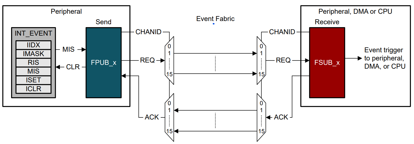
The event manager connects event publishers to event subscribers through an event fabric. There are three types of event fabric: CPU interrupt (Fixed event route), DMA route, and generic route. For example, Figure 3-4 shows the generic route.
GUID-51CEBA8B-869D-40DC-BEDB-09DBC71EC717-low.png

The event management register set contains 6 standard registers: RIS, IMASK, MIS, ISET, ICLR, and IIDX. And the event registers are interconnected as shown in Figure 3-5. Once unmasked, a pending interrupt is indicated in both the RIS and MIS registers, and an event is generated. In the case of a CPU interrupt with a CPU interrupt event route, a read of the IIDX register clears the highest priority pending interrupt in the RIS and MIS registers and return the index of the highest priority pending interrupt to application software.

Figure 3-4 Generic Event Route
GUID-04780062-7A56-4463-A295-853704783242-low.png Figure 3-5 Event Management Register Relationship

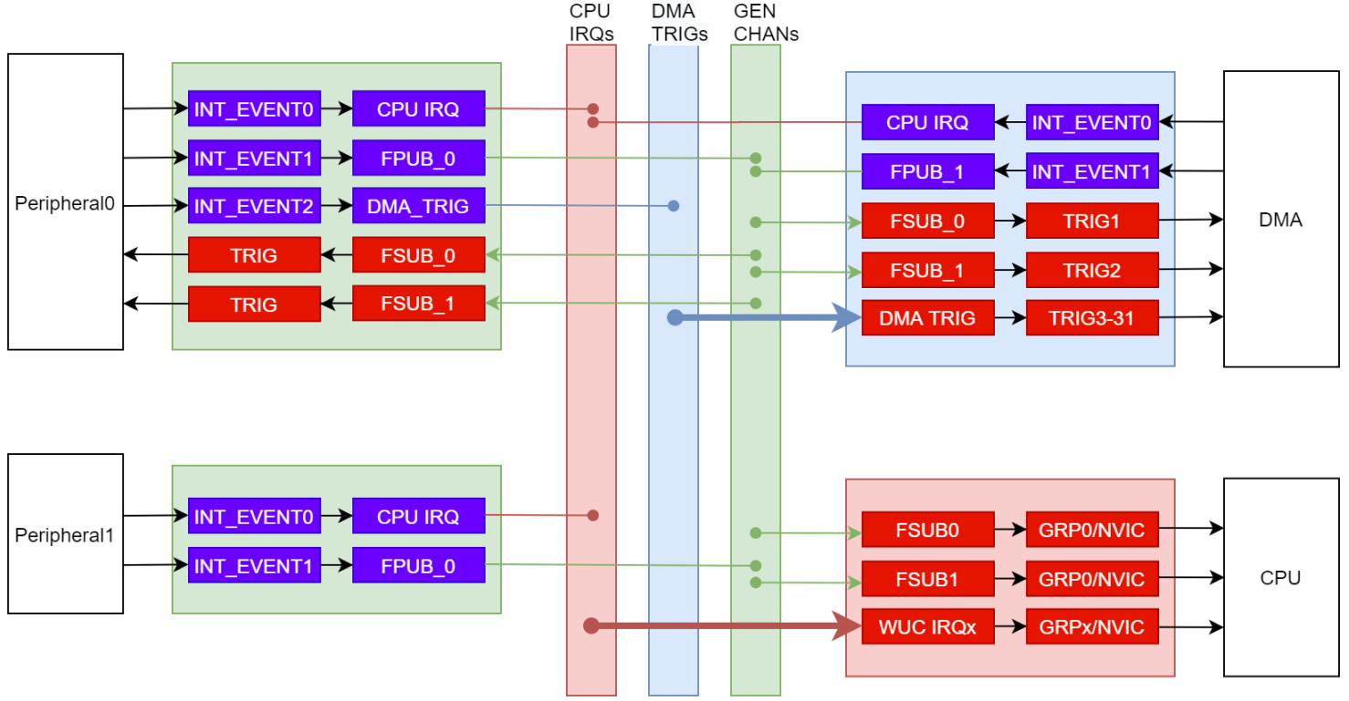
Figure 3-6 shows the event map. Different peripherals are routed through different event fabrics to achieve different event transitions. For more details on the use of the event handler in MSPM0, see the Event section of the MSPM0G technical reference manual, the MSPM0L technical reference manual, or the MSPM0C technical reference manual.
GUID-8319C6B2-E88C-412C-92AA-D82A6419F023-low.png Figure 3-6 MSPM0 Event and Interrupt Handling