SLAAEF9 November   2023 MSPM0L1306


  1.   1
  2.   Abstract
  3.   Trademarks
  4. 1MSPM0 Portfolio Overview
    1. 1.1 Introduction
    2. 1.2 Portfolio Comparison of Renesas RL78 MCUs to MSPM0 MCUs
  5. 2Ecosystem And Migration
    1. 2.1 Ecosystem Comparison
      1. 2.1.1 MSPM0 Software Development Kit (MSPM0 SDK)
      2. 2.1.2 The IDE Supported By MSPM0
      3. 2.1.3 SysConfig
      4. 2.1.4 Debug Tools
      5. 2.1.5 LaunchPad
    2. 2.2 Migration Process
      1. 2.2.1 Step 1. Choose The Right MSPM0 MCU
      2. 2.2.2 Step 2. Set Up IDE And Quick Introduction of CCS
        1. 2.2.2.1 Set Up IDE
        2. 2.2.2.2 Quick Introduction of CCS
      3. 2.2.3 Step 3. Set Up MSPM0 SDK And Quick Introduction of MSPM0 SDK
        1. 2.2.3.1 Set Up MSPM0 SDK
        2. 2.2.3.2 Quick Introduction of SDK
      4. 2.2.4 Step 4. Software Evaluation
      5. 2.2.5 Step 5. PCB Board Design
      6. 2.2.6 Step 6. Mass Production
    3. 2.3 Example
  6. 3Core Architecture Comparison
    1. 3.1 CPU
    2. 3.2 Embedded Memory Comparison
      1. 3.2.1 Flash Features
      2. 3.2.2 Flash Organization
        1. 3.2.2.1 Flash Memory Regions
        2. 3.2.2.2 NONMAIN Memory of MSPM0
        3. 3.2.2.3 Flash Memory Registers of RL78
      3. 3.2.3 Embedded SRAM
    3. 3.3 Power UP and Reset Summary and Comparison
    4. 3.4 Clocks Summary and Comparison
      1. 3.4.1 Oscillators
        1. 3.4.1.1 MSPM0 Oscillators
      2. 3.4.2 Clock Signal Comparison
    5. 3.5 MSPM0 Operating Modes Summary and Comparison
      1. 3.5.1 Operating Modes Comparison
      2. 3.5.2 MSPM0 Capabilities in Lower Modes
      3. 3.5.3 Entering Lower-Power Modes
      4. 3.5.4 Low-Power Mode Code Examples
    6. 3.6 Interrupts and Events Comparison
      1. 3.6.1 Interrupts and Exceptions
        1. 3.6.1.1 Interrupt Management of RL78
        2. 3.6.1.2 Interrupt Management of MSPM0
      2. 3.6.2 Event Handler of MSPM0
      3. 3.6.3 Event Link Controller (ELC) of RL78
      4. 3.6.4 Event Management Comparison
    7. 3.7 Debug and Programming Comparison
      1. 3.7.1 Debug Comparison
      2. 3.7.2 Programming Mode Comparison
        1. 3.7.2.1 Bootstrap Loader (BSL) Programming of MSPM0
        2. 3.7.2.2 Serial Programming (Using External Device) of RL78
  7. 4Digital Peripheral Comparison
    1. 4.1 General-Purpose I/O (GPIO, IOMUX)
    2. 4.2 Universal Asynchronous Receiver-Transmitter (UART)
    3. 4.3 Serial Peripheral Interface (SPI)
    4. 4.4 Inter-Integrated Circuit (I2C)
    5. 4.5 Timers (TIMGx, TIMAx)
    6. 4.6 Windowed Watchdog Timer (WWDT)
    7. 4.7 Real-Time Clock (RTC)
  8. 5Analog Peripheral Comparison
    1. 5.1 Analog-to-Digital Converter (ADC)
    2. 5.2 Comparator (COMP)
    3. 5.3 Digital-to-Analog Converter (DAC)
    4. 5.4 Operational Amplifier (OPA)
    5. 5.5 Voltage References (VREF)

Power UP and Reset Summary and Comparison

Both RL78 devices and MSPM0 devices have the minimum operating voltage and have modules in place to make sure that the device starts up properly by holding the device or portions of the device in a reset state. Table 3-5 shows a comparison on how this is done between the two families and what modules control the power up process and reset across the families.

Table 3-5 Summary and Comparison of Power Up
RL78 MSPM0
POR (Power-On Reset Circuit) (1) Rise detection: VDD>VPOR, POR reset signal is released
Fall detection: VDD<VPDR, POR reset signal is generated
Power-On Reset (POR) Rise detection: VDD>POR+, POR state is released, and bandgap reference and BOR is started
Fall detection: VDD<POR-, device is held in POR state
LVD (Voltage Detector)-Reset mode Rise detection: VDD>VLVD, LVD reset signal is released
Fall detection: VDD<VLVD, LVD reset signal is generated
Brownout Reset (BOR)- 0 level (2) Rise detection: VDD>BOR0+,
Device continues the boot process, and PMU is started
Fall detection: VDD<BOR0-,
Device is held in BOR state.
LVD (Voltage Detector)-Interrupt and reset mode Rise detection: VDD>VLVDH, LVD reset signal is released
Fall detection:
1) VDD<VLVDH: an interrupt request signal is generated
2) VDD<VLVDL: LVD reset signal is generated
Brownout Reset (BOR)- 1 to 3 level (2) Fall detection:
1) VDD<BORx- (x=1, 2, 3), an interrupt request is generated, and the BOR circuit automatically switches the BOR threshold level to BOR0.
2) VDD<BOR0-, Device is held in BOR state
LVD (Voltage Detector)-Interrupt mode Rise detection: VDD>VLVD, LVD reset signal is released
After the LVD reset is released, an interrupt request signal is generated when VDD>VLVD or VDD<VLVD
N/A N/A
RTCPOR (RTC Power-on Reset) Reset of the RTC and XT1 oscillator by comparison of supply voltage of the RTCPOR circuit and detection voltage RTC and associated clocks are reset through BOOTRST, BOR, or POR
Some RL78 devices have SPOR (Selectable Power-On Reset Circuit) whose detection level for the power supply detection can be selected by using the option byte.
There are four selectable BOR threshold levels (BOR0-BOR3). During startup, the BOR threshold is always BOR0 (the lowest value) to make the device always starts at the specified VDD minimum. After boot, software can optionally re-configure the BOR circuit to use a different (higher) threshold level.

The relationship between various voltage thresholds of RL78 is: VPDR < VPOR <Low limit of operation voltage < VLVDL < VLVDH. The relationship between various voltage thresholds of MSPM0 is: POR- < POR+ < BOR0- < BOR0+, and BOR0+ is the specified VDD minimum to enable correct operation of internal circuits.

Figure 3-1 shows the MSPM0 Reset function. MSPM0 devices have five reset levels: Power-on reset (POR), Brownout reset (BOR), Boot reset (BOOTRST), System reset (SYSRST) and CPU reset (CPURST).
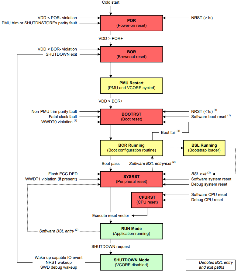
GUID-5E59ED64-D36E-4318-AC01-FC16699170CF-low.png Figure 3-1 MSP Reset Function