SLAU278AH May 2009 – March 2021
- 1Read This First
-
1Get Started Now!
- 1.1 Kit Contents, MSP-TS430xx
- 1.2 Kit Contents, MSP-FET430xx
- 1.3 Kit Contents, MSP-FET
- 1.4 Kit Contents, MSP-FET430UIF
- 1.5 Kit Contents, MSP-FET430PIF
- 1.6 Kit Contents, eZ430-F2013
- 1.7 Kit Contents, eZ430-T2012
- 1.8 Kit Contents, eZ430-RF2500
- 1.9 Kit Contents, eZ430-RF2500T
- 1.10 Kit Contents, eZ430-RF2500-SEH
- 1.11 Kit Contents, eZ430-Chronos-xxx
- 1.12 Kit Contents, FET430F6137RF900
- 1.13 Kit Contents, EM430Fx1x7RF900
- 1.14 Hardware Installation, MSP-FET and MSP-FET430UIF
- 1.15 Hardware Installation, MSP-TS430xxx, MSP-FET430Uxx, FET430F6137RF900, EM430Fx1x7RF900
- 1.16 Hardware Installation, eZ430-XXXX, MSP-EXP430G2, MSP-EXP430FR5739, MSPEXP430F5529
- 1.17 Important MSP430 Documents on the Web
-
2Design Considerations for In-Circuit Programming
- 2.1 Signal Connections for In-System Programming and Debugging
- 2.2 External Power
- 2.3
Bootloader (BSL)
-
A Frequently Asked Questions and Known Issues
- A.1 Hardware FAQs
-
A.2 Known Issues
- MSP-FET430UIF
-
MSP-FET430PIF
-
B Hardware
- B.1 MSP-TS430D8
- B.2 MSP-TS430PW14
- B.3 MSP-TS430L092
- B.4 MSP-TS430L092 Active Cable
- B.5 MSP-TS430PW20
- B.6 MSP-TS430RHL20
- B.7 MSP-TS430PW24
- B.8 MSP-TS430RGE24A
- B.9 MSP-TS430DW28
- B.10 MSP-TS430PW28
- B.11 MSP-TS430PW28A
- B.12 MSP-TS430RHB32A
- B.13 MSP-TS430DA38
- B.14 MSP-TS430QFN23x0
- B.15 MSP-TS430RSB40
- B.16 MSP-TS430RHA40A
- B.17 MSP-TS430DL48
- B.18 MSP-TS430PT48
- B.19 MSP-TS430PT48A
- B.20 MSP-TS430RGZ48B
- B.21 MSP-TS430RGZ48C
- B.22 MSP-TS430PM64
- B.23 MSP-TS430PM64A
- B.24 MSP-TS430PM64D
- B.25 MSP-TS430PM64F
- B.26 MSP-TS430RGC64B
- B.27 MSP-TS430RGC64C
- B.28 MSP-TS430RGC64USB
- B.29 MSP-TS430PN80
- B.30 MSP-TS430PN80A
- B.31 MSP-TS430PN80B
- B.32 MSP-TS430PN80C
- B.33 MSP-TS430PN80USB
- B.34 MSP-TS430PZ100
- B.35 MSP-TS430PZ100A
- B.36 MSP-TS430PZ100B
- B.37 MSP-TS430PZ100C
- B.38 MSP-TS430PZ100D
- B.39 MSP-TS430PZ100E
- B.40 MSP-TS430PZ5x100
- B.41 MSP-TS430PZ100USB
- B.42 MSP-TS430PZ100AUSB
- B.43 MSP-TS430PEU128
- B.44 EM430F5137RF900
- B.45 EM430F6137RF900
- B.46 EM430F6147RF900
-
B Hardware
-
A Frequently Asked Questions and Known Issues
B.27 MSP-TS430RGC64C
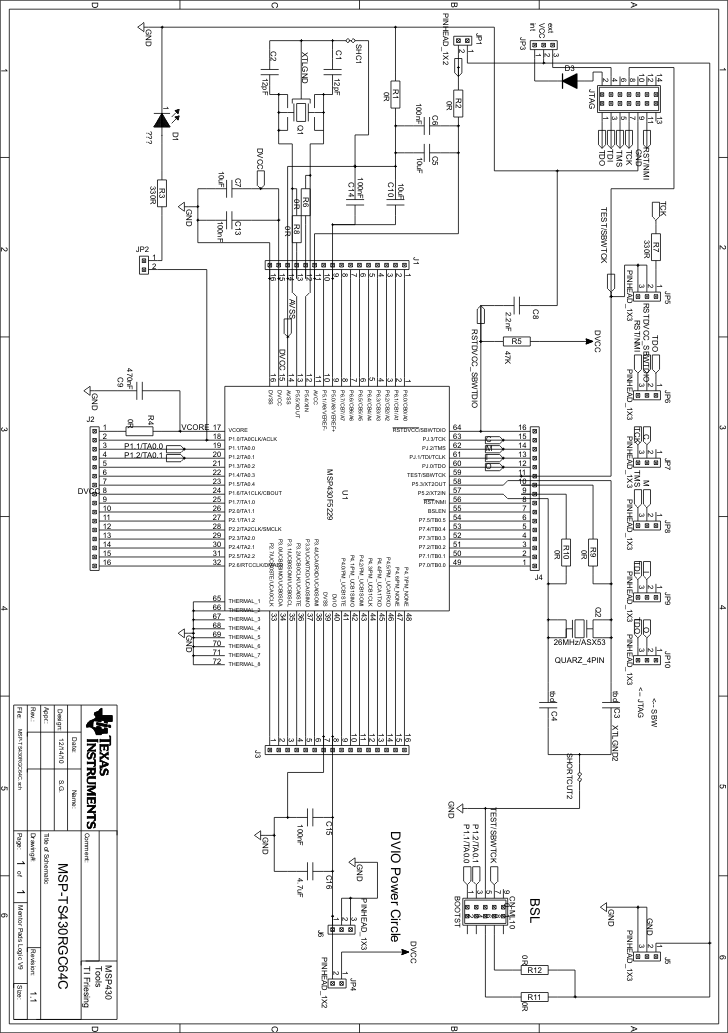
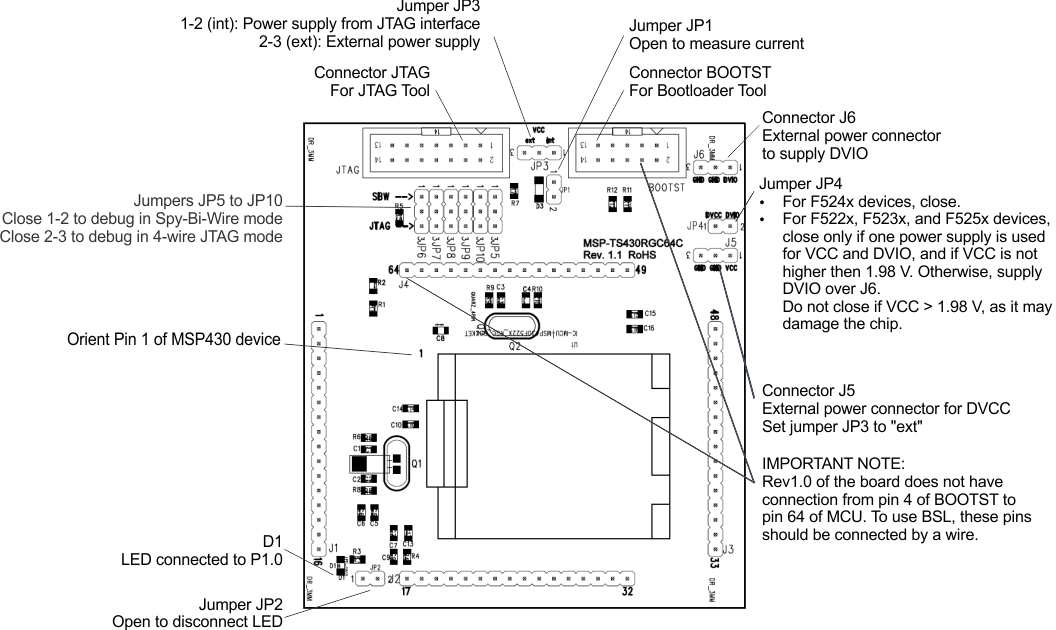
The MSP-TS430RGC64C target board has been designed with the option to operate with the target device DVIO input voltage supplied via header J6 (see Figure 5-54). This development platform does not supply the 1.8-V DVIO rail on board and it MUST be provided by external power supply for proper device operation. For correct JTAG connection, programming, and debug operation, it is important to follow this procedure:
- Make sure that the VCC and DVIO voltage supplies are OFF and that the power rails are fully discharged to 0 V.
- Enable the 1.8-V external DVIO power supply.
- Enable the 1.8-V to 3.6-V VCC power supply (alternatively, this supply can be provided from the MSP-FET430UIF JTAG debugger interface).
- Connect the MSP-FET430UIF JTAG connector to the target board.
- Start the debug session using IAR or CCS IDE.
For more information on debugging the MSP430F522x and MSP430F525x, see the device-specific data sheets (MSP430F522x and MSP430F525x) and Designing with MSP430F522x and MSP430F521x Devices.
For debugging of devices (MSP430F524x and MSP430F523x) without use of the DVIO power domain, short JP4 with the jumper.
 Figure 4-54 MSP-TS430RGC64C Target Socket Module, Schematic
 Figure 4-55 MSP-TS430RGC64C Target Socket Module, PCB
For bootloader use, the BSL connector and only one of the resistors R11 or R12 must be populated. If the board is supplied internally, R11 (0 Ω) must be assembled. If the board is supplied externally, R12 (0 Ω) must be assembled, and R11 must be removed.
| Item | Qty | Reference | Value | Description | Comment | Supplier No. |
|---|---|---|---|---|---|---|
| 1 | 0 | C1, C2 | 12pF | CAP, SMD, Ceramic, 0805 | DNP C1 C2 | |
| 2 | 0 | C3, C4 | CAP, SMD, Ceramic, 0805 | DNP C3 C4 | ||
| 4 | 3 | C5, C7, C10 | 10uF | CAP, SMD, Ceramic, 0805 | ||
| 5 | 5 | C8 C6 C13-15 | 100nF | CAP, SMD, Ceramic, 0805 | Digi-Key: 311-1245-2-ND | |
| 5 | 5 | C8 | 2.2nF | CAP, SMD, Ceramic, 0805 | ||
| 6 | 1 | C9 | 470nF | CAP, SMD, Ceramic, 0805 | Digi-Key: 478-1403-2-ND | |
| 7 | 1 | C16 | 4.7uF | CAP, SMD, Ceramic, 0805 | ||
| 8 | 1 | D1 | Green LED | LED, SMD, 0805 | ||
| 9 | 4 | J1-J4 | 16-pin header | Pin header 1x16: Grid: 100mil (2.54 mm) | DNP: headers and receptacles enclosed with kit. Keep vias free of solder. : Header : Receptacle | SAM1029-16-ND SAM1213-16-ND |
| 10 | 2 | J5, J6 | 3-pin header, male, TH | Pin header 1x3: Grid: 100mil (2.54 mm) | SAM1035-03-ND | |
| 11 | JP5, JP6, JP7, JP8, JP9, JP10 | 3-pin header, male, TH | Pinheader 1x3: Grid: 100mil (2.54 mm) | place jumpers on pins 2-3 | SAM1035-03-ND | |
| 12 | JP3 | 3-pin header, male, TH | Pin header 1x3: Grid: 100mil (2.54 mm) | place jumper on pins 1-2 | SAM1035-03-ND | |
| 13 | JP1, JP2, JP4 | 2-pin header, male, TH | Pin header 1x2; Grid: 100mil (2.54 mm) | place jumper on header | SAM1035-02-ND | |
| 14 | 10 | Jumper | Place on: JP1, JP2, JP3, JP4, JP5, JP6, JP7, JP8, JP9, JP10 | 15-38-1024-ND | ||
| 15 | 1 | JTAG | 2x7Pin,Wanne | Header, THD, Male 2x7 Pin, Wanne, 100mil spacing | HRP14H-ND | |
| 16 | 0 | BOOTST | 2x5Pin,Wanne | Header, THD, Male 2x5 Pin, Wanne, 100mil spacing | DNP | |
| 17 | 1 | Q1 | 26MHz/ASX53 | CRYSTAL, SMD, 5x3MM, 26MHz | Only Kit. | |
| 18 | 0 | Q2 | 26MHz/ASX53 | CRYSTAL, SMD, 5x3MM, 26MHz | 300-8219-1-ND | |
| 19 | 1 | D3 | LL103A | DIODE, SMD, SOD123, Schottky | Buerklin: 24S3406 | |
| 20 | 2 | R3, R7 | 330 Ohm, SMD0805 | 541-330ATR-ND | ||
| 21 | 1 | R5 | 47k Ohm, SMD0805 | RES, SMD, 0805, 1/8W, x% | 541-47000ATR-ND | |
| 22 | R1, R2, R4, R6, R8, R9, R10, R11, R12 | 0 Ohm, SMD0805 | RES, SMD, 0805, 1/8W, x% | DNP: R6, R8, R9, R10, R11,R12 | 541-000ATR-ND | |
| 23 | 1 | U1 | Socket: QFN11T064-006-N-HSP | Manuf.: Yamaichi | ||
| 24 | 2 | MSP430 | MSP430F5229IRGCR | IC, MCU, SMD, 9.15x9.15mm Thermal Pad with Socket | ||
| 25 | 4 | Rubber stand off | Rubber stand off | apply to corners at bottom side | Buerklin: 20H1724 | |
| 26 | 1 | PCB | 84 x 76 mm | 84 x 76 mm |