SLUT008 November 2023 LMG3612 , LMG3614 , LMG3616 , LMG3622 , LMG3624 , LMG3626
TI's latest family of high-voltage, low-power GaN FETs; LMG3622, LMG3624, and LMG3626, provide simplicity and integration for high power density applications in a wide range of end equipment such as charging adapters, TV power supplies, server auxiliary power supplies, and more. As GaN-based power supply designs continue to become more prevalent for their efficiency and size benefits, the integration and feature set provided by TI GaN enable system improvements such as BOM count reduction, board area reduction, and better thermal management. This product overview explains key features supported with empirical data as well as design guidelines for working with TI's LMG362x family of GaN devices.
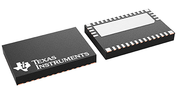
 Figure 1 LMG362x Device Package
General Feature Overview
- An integrated gate driver reduces component count and simplifies design, while greatly reducing the parasitic loop inductance.
- Current-sense emulation (lossless current sensing) greatly reduces the size and power losses of traditional current-sense resistors.
- Low quiescent current consumption enables low standby power, as mandated by CoC and DoE requirements. Device quiescent current consumption is further reduced by setting the EN pin low.
- Device protections like overcurrent protection (OCP), overtemperature protection (OTP), and undervoltage lockout (UVLO) provide system-level reliability against system faults.
- Device pinout provides a clear separation between signal and power connections, enabling an easy layout for the switching loop.
 Figure 2 LMG362x Device Feature
Overview
Figure 2 LMG362x Device Feature
OverviewThe LMG362x family of devices is available in a 8-mm × 5.3-mm QFN package with a source-connected thermal pad. With a 650-V rating, a wide (10 V–26 V) AUX supply and IN voltage range, the device can plug and play in a variety of applications. Coming in three different variations of RDS(on) values, the device can be optimized between power loss and cost depending on the power level of the application. The integrated gate driver reduces component count and simplifies design, while greatly reducing the parasitic switching and gating loop inductance. Current-sense emulation (lossless current sensing) greatly reduces the size and power losses of traditional current-sense resistors. Low quiescent current consumption enables low standby power, as mandated by European Code of Conduct (CoC) and North American Department of Energy (DoE) requirements; device quiescent current consumption is further reduced by setting the EN pin low. Device protections like OCP, OTP, and UVLO provide system-level reliability against system faults. Finally, the device pinout provides a clear separation between signal and power connections, enabling an easy layout for the switching loop.
Integrated Current Sensing (Lossless Current Sensing)
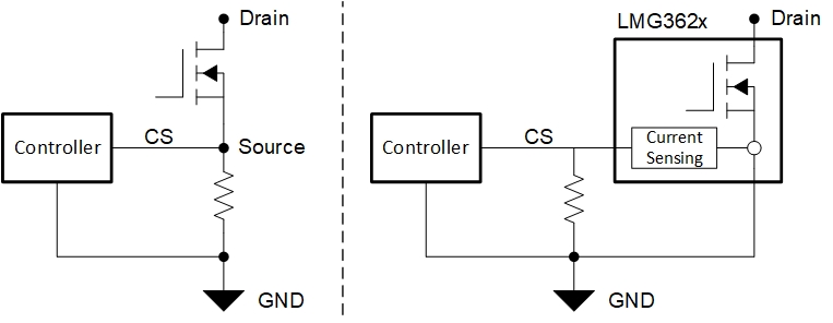
Applications that require current sensing have traditionally used a series shunt resistor between the source of the switching device and the system ground. This traditional current-sensing method is undesirable as this method requires a physically large sensing resistor, RCS(trad), that dissipates significant power, adding unwanted heat to the system and reducing the overall efficiency. Additionally, with this sensing method, the source of the device is separated from the system ground, making it difficult to connect the thermal pad to a large ground plane which is desirable for better thermal dissipation. The LMG362x family of devices addresses all the complexities of traditional current sensing with the integrated current-sense emulation feature. The feature works as follows:
- The CS pin on the LMG362x device outputs a scaled-down copy of the drain-source current.
- This current is then fed through a physically small resistor, Rcs, to create the current-sense voltage required by the system controller.
 Figure 3 Traditional Current Sensing vs
Integrated Current Sensing Connections
Figure 3 Traditional Current Sensing vs
Integrated Current Sensing ConnectionsThe RCS resistor value is selected as follows:
where
Gcse is the current-sense gain of the LMG362x device, as specified in Table 1.
| Device | Gcse |
|---|---|
| LMG3622 | 0.691 mA/A |
| LMG3624 | 0.965 mA/A |
| LMG3626 | 1.633 mA/A |
Because the current sensed by the resistor is scaled down by a large factor, the power dissipation in Rcs is minimal compared to the traditional current-sensing method. Figure 4 shows the power loss comparison across load in the case of a 100-W flyback converter.
 Figure 4 Power Loss Comparison of
Traditional Current Sensing vs Integrated Current Sensing
Figure 4 Power Loss Comparison of
Traditional Current Sensing vs Integrated Current SensingFor more information and empirical data on the current-sense emulation feature of LMG362x , see the Maximize System Efficiency With Integrated Current Sensing from TI GaN application brief.
Low Quiescent Current and Standby Mode
As DoE Level VI and CoC Tier 2 requirements for standby and light-load power consumption continue to grow more stringent over time, new power-supply designs must consider the impact of integrated circuit (IC) power dissipation.
The LMG362x family of devices have a quiescent current consumption of 240 μA when EN is set high and 50 μA when EN is set low. Low quiescent currents support converter burst-mode operation that is critical for meeting the light-load efficiency mandates. The EN pin can be interfaced to any type of control methodology which optimizes standby power at very light or no-load conditions.
| Parameter | Quiescent Current Consumption | Device Power Loss (AUX = 15 V) |
|---|---|---|
| EN pin = high | 240 μA | 3.6 mW |
| EN pin = low | 50 μA | 0.75 mW |
As an example, LMG3624EVM-081, is able to achieve a combined 70 mW of no-load standby
power at
VIN = 230 Vac.
Device Protections
For additional system reliability and robustness, LMG362x devices are equipped with both OCP and overtemperature protection OTP. These features make sure that the GaN Power FET device is protected from abnormal system faults. The OCP operation is implemented with a cycle-by-cycle scheme as shown in Figure 5. If the FET current exceeds the IT(OC) threshold value while IN is high, the FET is automatically turned off for the remainder of the IN-high period. The next time that IN goes high, the FET turns on and checks for an overcurrent condition again.
 Figure 5 LMG362x Cycle-by-Cycle
Overcurrent Protection Operation
Figure 5 LMG362x Cycle-by-Cycle
Overcurrent Protection OperationThe overcurrent threshold per device is shown in Table 3.
| Device | IT(OC) (typical) |
|---|---|
| LMG3622 | 8.5 A |
| LMG3624 | 6 A |
| LMG3626 | 3.6 A |
The OTP operation makes sure that the FET is held off when the LMG362x temperature is above the OTP threshold of 165 degrees. A hysteresis band of 20 degrees makes sure that erroneous thermal cycling is prevented. Furthermore, the OTP condition is reported by the active-low FLT pin which can be interfaced to the system controller.
Turn-On Slew Rate Setting
To give system designers flexibility in optimizing between power losses or reduced common-mode EMI signatures, the LMG362x devices provide a programmable RDRV pin, which sets the turn-on slew rate of the FET.
| Turn-On Slew Rate Setting |
Recommended Typical Programming Resistance (kΩ) | Typical Turn-on Slew Rate (V/ns) | Comment |
|---|---|---|---|
| 0 (slowest) | 120 | 20 | Open-circuit connection for programming resistance is acceptable |
| 1 | 47 | 50 | |
| 2 | 22 | 75 | |
| 3 (fastest) | 5.6 | 150 | Short-circuit connection for programming resistance (RDRV shorted to AGND) is acceptable |
Actual VDS waveforms for different slew rate settings are shown in Figure 6.
 Figure 6 Drain-Source Voltage Data for
Different Slew-Rate Settings
Figure 6 Drain-Source Voltage Data for
Different Slew-Rate SettingsPackage Pinout Advantage and Layout Recommendations
The LMG362x package pinout is configured with a clear separation between signal pins and power pins, enabling a simple layout where the power path remains interrupted. As shown in Figure 7, there is a distinct separation between the drain pins, source pins, thermal pad, and all other signal pins (RDRV, AUX, FLT, AGND, IN).
 Figure 7 LMG362x Pin
Configuration
Figure 7 LMG362x Pin
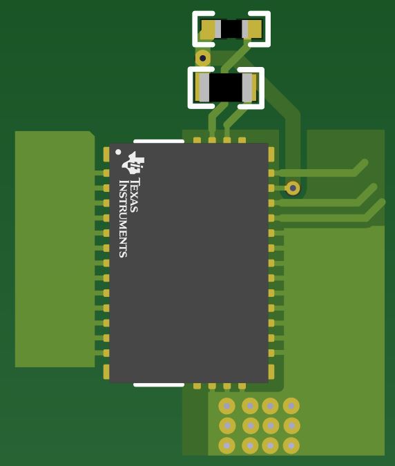
ConfigurationWith this configuration, a simple layout is achieved where the copper pour for the source can be extended to the right and bottom of the PCB, with no interruptions, as shown in Figure 8.
 Figure 8 LMG362x Layout With Separation
Between Drain, Source, and Signal Connections
Figure 8 LMG362x Layout With Separation
Between Drain, Source, and Signal ConnectionsThis continuity in the source connection increases the total PCB area that can be connected to the thermal pad.