SLYT816 October 2021 TPS548B27 , TPS548B28
7 Switch-node ringing comparison
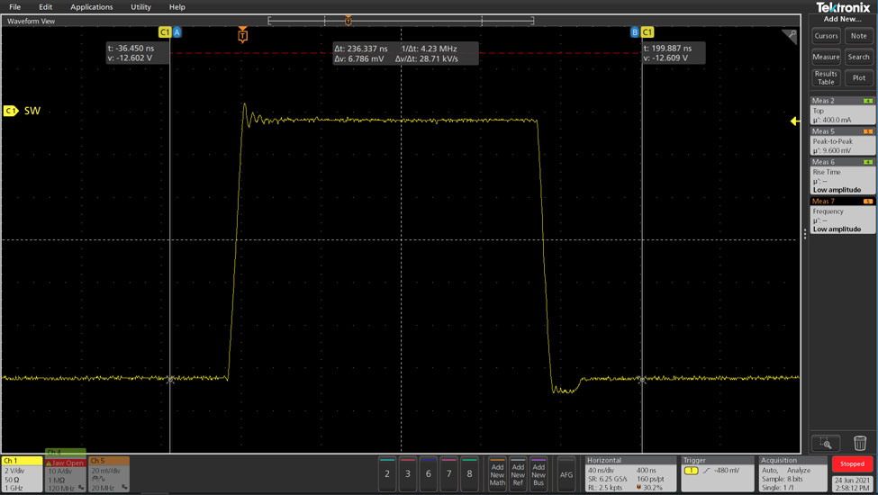
The effects of parasitic inductance are visible when observing the switch-note ringing of the power supply’s high-side MOSFET. Under close inspection of Figure 7-1 and Figure 7-2, the voltage overshoot of the Enhanced HotRod QFN package design was 0.1 V lower than the HotRod package design shown in Table 7-1, which is noticeable. It is difficult to ascertain where the difference in voltage ringing originates, but it is safe to assume that the Enhanced HotRod QFN package does not degrade switch-node ringing performance. It is probable, however, that mechanical construction of the Enhanced HotRod QFN package slightly improves switch-node ringing of the high-side MOSFET by reducing the internal parasitic inductance of the IC.
| Package | VIN | VOUT | FSW | Ringing |
|---|---|---|---|---|
| Enhanced HotRod QFN package | 12 V | 1 V | 600 kHz | 0.7 V |
| HotRod package | 0.8 V |
 Figure 7-1 Enhanced HotRod QFN package
high-side FET ringing
 Figure 7-2 HotRod package high-side FET
ringing