SLYT816 October 2021 TPS548B27 , TPS548B28
2 Design considerations
The Enhanced HotRod QFN package includes a more flexible layout, which gives you the ability to place external components closer to the integrated circuit (IC) and reduce parasitic effects by improving the interconnect between the die and the leadframe. Increasingly, semiconductor manufacturers are designing DC/DC converters for smaller circuits, with tighter spacing inside the DC/DC converter, and in smaller packages. As such, a multilayer leadframe offers design advantages and flexibility inside the IC compared to a single-layer leadframe. For this comparison, we used an Enhanced HotRod QFN package DC/DC converter with a 0.5-mm pin pitch to more easily accommodate soldering manufacturing preferences and board-level reliability requirements.
To demonstrate the performance of each package type, we designed and built two different power supplies, attempting to make the design and operating conditions of each power supply as identical as possible. We selected the 16-V, 20-A TPS548B27 and TPS548B28 synchronous buck converters for the comparison. Both are available in 3-mm-by-4-mm QFN packages. The only difference between the two devices is the mechanical construction of each package.
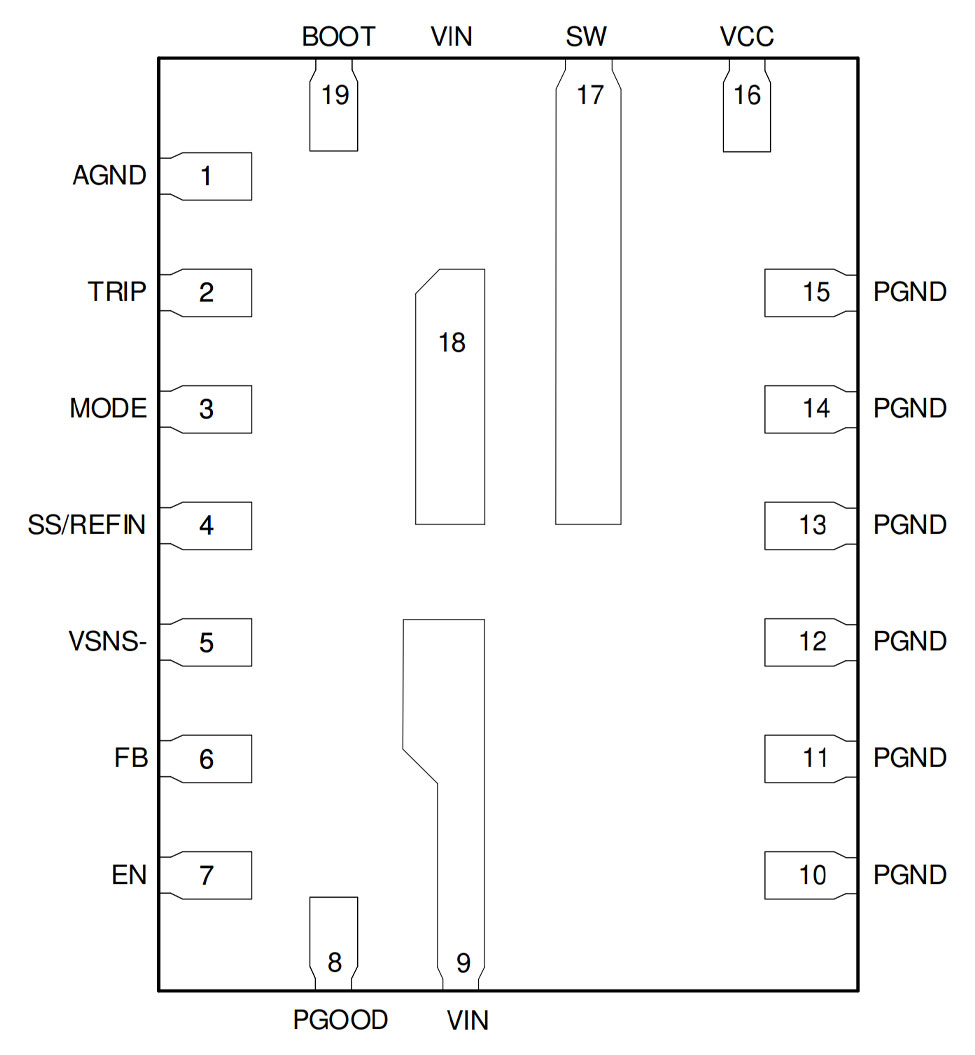
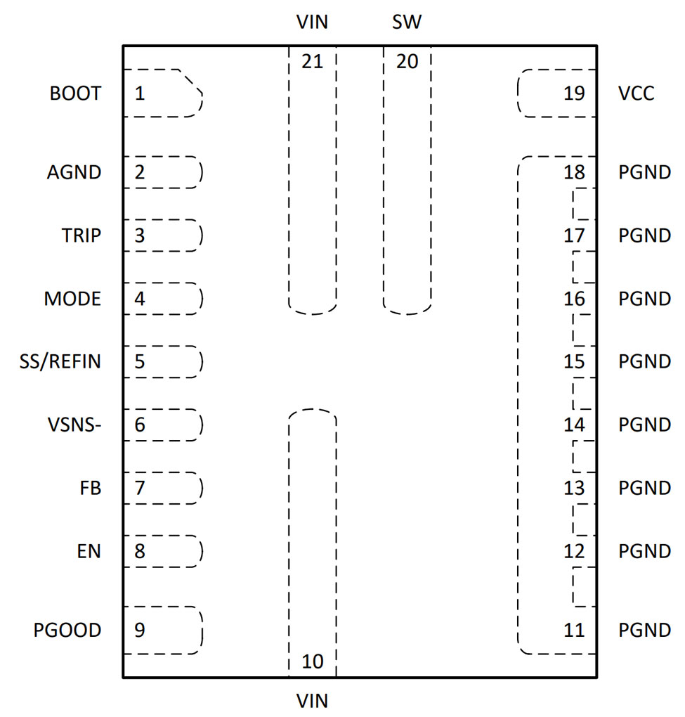
Figure 2-1 shows the TPS548B27 19-pin Enhanced HotRod QFN package with a 0.5-mm pin pitch. Figure 2-2 shows the TPS548B28 21-pin HotRod package with a 0.4-mm pin pitch. Close inspection of the pinout shows the same circuit integrated into each package. We moved several pins to the smaller sides of the Enhanced HotRod QFN package to accommodate a 0.5-mm pin pitch, and reduced the number of PGND pins. This change was made possible by the Enhanced HotRod QFN without metal rework of the die, and is a good example demonstrating the flexibility of this new package technology.
For each design, the input voltage is 12 V, the output voltage is 1 V and the output current for each device is capable of 20 A. These requirements are typical for powering a high-performance processor such as a high-current field-programmable gate array or an application-specific integrated circuit processor. A 600-kHz switching frequency was chosen for each power supply, and both designs use the Coilcraft XAL7070-301MEB inductor rated at 300 nH with a DC resistance of 1.06 mΩ. Each design also uses the same amount of ceramic input and output capacitance, in order to optimize the designs for high power density and a small solution size.
 Figure 2-1 Enhanced HotRod QFN package
example (top view)
 Figure 2-2 HotRod package example (top
view)