SLYT816 October 2021 TPS548B27 , TPS548B28
3 Layout comparison
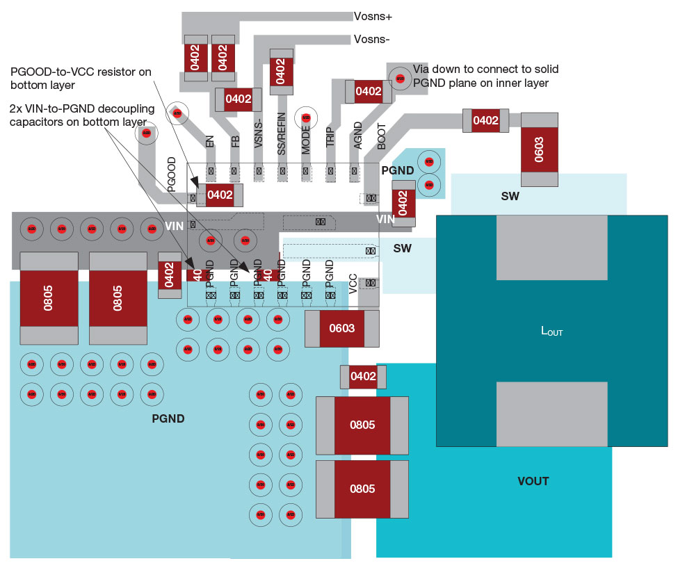
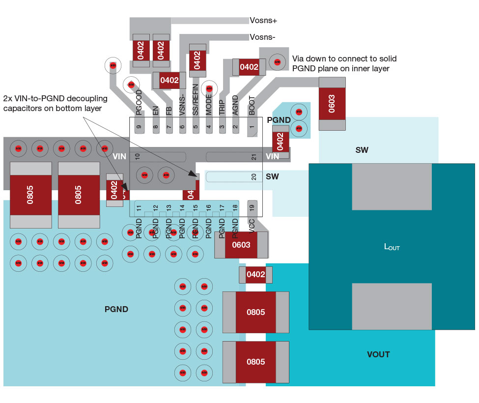
Figure 3-1 shows the circuit board layout for the Enhanced HotRod QFN package. Figure 3-2 shows the layout for the HotRod package. The evaluation module is laid out in a manner typical of a user application, with the top, bottom and internal layers using 2-ounce copper. The top-side ground traces are connected to the bottom and internal ground planes with multiple via groupings placed around the board. The input decoupling capacitors and bootstrap capacitor are all located as close to the IC as possible in each design. An additional input bulk capacitor was used to limit the noise entering the converter from the input supply, and terminated critical noise-sensitive analog circuits to the quiet analog ground island on the top layer. The layout of each design is very similar, in order to make it easier to detect any difference in performance between the two packages.
 Figure 3-1 Enhanced HotRod QFN package
layout
 Figure 3-2 HotRod package layout