SNAU246A June   2020  – January 2021 LMX2820


  1. 1Trademarks
  2. 2LMX2820EVM Evaluation Module
    1. 2.1 Evaluation Module Contents
    2. 2.2 Evaluation Setup Requirement
    3. 2.3 Resources
  3. 3Setup
    1. 3.1 Connection Diagram
    2. 3.2 Power Supply
    3. 3.3 Reference Clock
    4. 3.4 RF Output
    5. 3.5 Programming
    6. 3.6 Evaluation Software
  4. 4Typical Measurement
    1. 4.1 Default Configuration
      1. 4.1.1 Loop Filter
      2. 4.1.2 Typical Output
    2. 4.2 Additional Tests
      1. 4.2.1 SYSREF Example
      2. 4.2.2 Offset Mixing With PFDIN Pin
      3. 4.2.3 External VCO Mode
      4. 4.2.4 Register Readback
  5. 5Schematic
  6. 6PCB Layout and Layer Stack-Up
    1. 6.1 PCB Layer Stack-Up
    2. 6.2 PCB Layout
  7. 7Bill of Materials
  8. 8Troubleshooting Guide
    1.     A Using Different Reference Clock
      1.      B USB2ANY Firmware Upgrade
        1.       C Revision History

Using Different Reference Clock

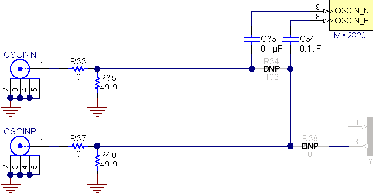
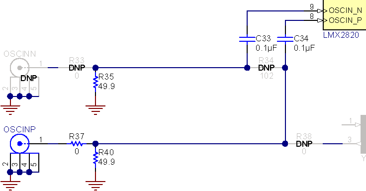
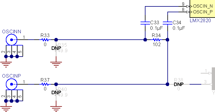
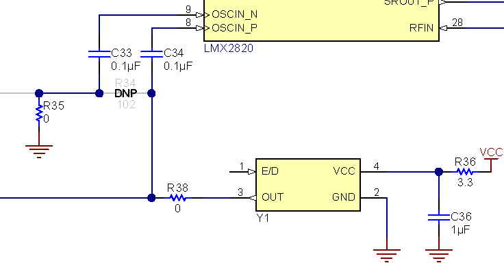
These are the different options to provide a reference clock to LMX2820EVM. By default, the EVM is configured for an external single-ended clock.
Table A-1 Reference Clock Input Configuration
DIFFERENTIAL CLOCK SINGLE-ENDED CLOCK
GUID-E437B1B9-1821-4E8C-9102-37271CEA13CA-low.png GUID-28293B6E-50D2-43B0-8355-526A17A56BC1-low.png
GUID-F0CFC63E-B4BE-468D-8EAC-6252EF9BCDB8-low.png GUID-FF949F7B-108E-404C-9215-605059500412-low.png